

Viz Specifikace pro podrobnosti o produktu.
XC6118N09CGR-G
Product Overview
Category
XC6118N09CGR-G belongs to the category of voltage regulators.
Use
It is primarily used for regulating voltage in electronic circuits.
Characteristics
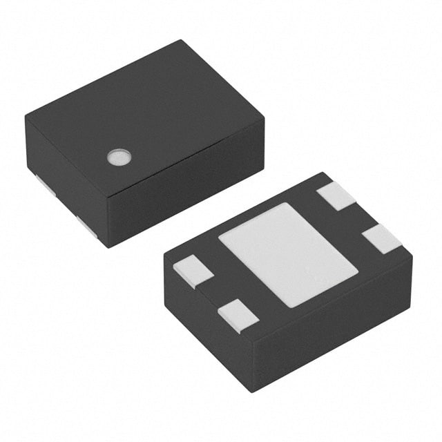
- Package: CGR (SOT-89)
- Essence: Low dropout voltage regulator
- Packaging/Quantity: Tape and reel, 3000 pieces per reel
Specifications
The specifications of XC6118N09CGR-G are as follows:
- Input Voltage Range: 2.5V to 6.0V
- Output Voltage: 0.9V
- Dropout Voltage: 200mV at 100mA
- Output Current: 100mA
- Quiescent Current: 30µA
- Line Regulation: ±0.1%
- Load Regulation: ±0.3%
- Operating Temperature Range: -40°C to +85°C
Detailed Pin Configuration
XC6118N09CGR-G has the following pin configuration:
- VIN (Input Voltage)
- GND (Ground)
- VOUT (Output Voltage)
Functional Features
The functional features of XC6118N09CGR-G include:
- Low dropout voltage
- Low quiescent current
- High output accuracy
- Overcurrent protection
- Thermal shutdown protection
Advantages and Disadvantages
Advantages: - Low dropout voltage ensures efficient power conversion. - Low quiescent current minimizes power consumption. - High output accuracy provides stable voltage regulation. - Overcurrent protection safeguards the circuit from damage. - Thermal shutdown protection prevents overheating.
Disadvantages: - Limited output current capacity (100mA). - Restricted input voltage range (2.5V to 6.0V).
Working Principles
XC6118N09CGR-G works by regulating the input voltage to a stable output voltage of 0.9V. It achieves this by utilizing a feedback mechanism that continuously adjusts the internal circuitry to maintain the desired output voltage, even in the presence of varying input voltages and load conditions.
Detailed Application Field Plans
XC6118N09CGR-G finds applications in various electronic devices and systems, including but not limited to:
- Battery-powered devices
- Portable electronics
- IoT (Internet of Things) devices
- Wearable technology
- Embedded systems
Detailed and Complete Alternative Models
Some alternative models that can be considered as alternatives to XC6118N09CGR-G are:
- XC6206P092MR-G
- LM1117IMPX-0.9/NOPB
- MCP1700T-0902E/TT
These models offer similar functionality and specifications, providing options for designers based on their specific requirements.
In conclusion, XC6118N09CGR-G is a low dropout voltage regulator used for voltage regulation in electronic circuits. Its key features include low dropout voltage, low quiescent current, high output accuracy, and protection mechanisms. It is suitable for various applications in battery-powered devices, portable electronics, IoT devices, wearable technology, and embedded systems. Alternative models such as XC6206P092MR-G, LM1117IMPX-0.9/NOPB, and MCP1700T-0902E/TT can also be considered.
Seznam 10 běžných otázek a odpovědí souvisejících s aplikací XC6118N09CGR-G v technických řešeních
Sure! Here are 10 common questions and answers related to the application of XC6118N09CGR-G in technical solutions:
Q: What is XC6118N09CGR-G? A: XC6118N09CGR-G is a voltage detector IC (integrated circuit) that monitors the power supply voltage and provides a reset signal when the voltage drops below a certain threshold.
Q: What is the operating voltage range of XC6118N09CGR-G? A: The operating voltage range of XC6118N09CGR-G is typically between 0.9V and 6.0V.
Q: How does XC6118N09CGR-G help in technical solutions? A: XC6118N09CGR-G helps in technical solutions by providing a reliable reset signal to microcontrollers, microprocessors, or other digital circuits when the power supply voltage falls below a specified level.
Q: Can XC6118N09CGR-G be used in battery-powered applications? A: Yes, XC6118N09CGR-G can be used in battery-powered applications as it has a low quiescent current consumption, making it suitable for power-sensitive designs.
Q: What is the typical reset voltage threshold of XC6118N09CGR-G? A: The typical reset voltage threshold of XC6118N09CGR-G is 0.9V.
Q: Does XC6118N09CGR-G have an adjustable reset voltage threshold? A: No, XC6118N09CGR-G has a fixed reset voltage threshold and does not offer adjustable options.
Q: What is the output type of XC6118N09CGR-G? A: XC6118N09CGR-G has an open-drain output type, which requires an external pull-up resistor.
Q: What is the maximum supply current of XC6118N09CGR-G? A: The maximum supply current of XC6118N09CGR-G is typically 1.5µA.
Q: Can XC6118N09CGR-G tolerate voltage spikes or transients? A: Yes, XC6118N09CGR-G has built-in hysteresis to tolerate voltage spikes and transients, ensuring stable operation.
Q: Is XC6118N09CGR-G available in different package options? A: Yes, XC6118N09CGR-G is available in various package options, such as SOT-25 and USP-4B, providing flexibility for different PCB layouts and space constraints.
Please note that the answers provided here are general and may vary depending on the specific datasheet and manufacturer's specifications of XC6118N09CGR-G.