Viz Specifikace pro podrobnosti o produktu.

XC6121F618MR-G
Product Overview
Category
XC6121F618MR-G belongs to the category of voltage regulators.
Use
It is commonly used in electronic circuits to regulate and stabilize voltage levels.
Characteristics
- Voltage regulation
- Stabilization of voltage levels
- Compact size
- Low power consumption
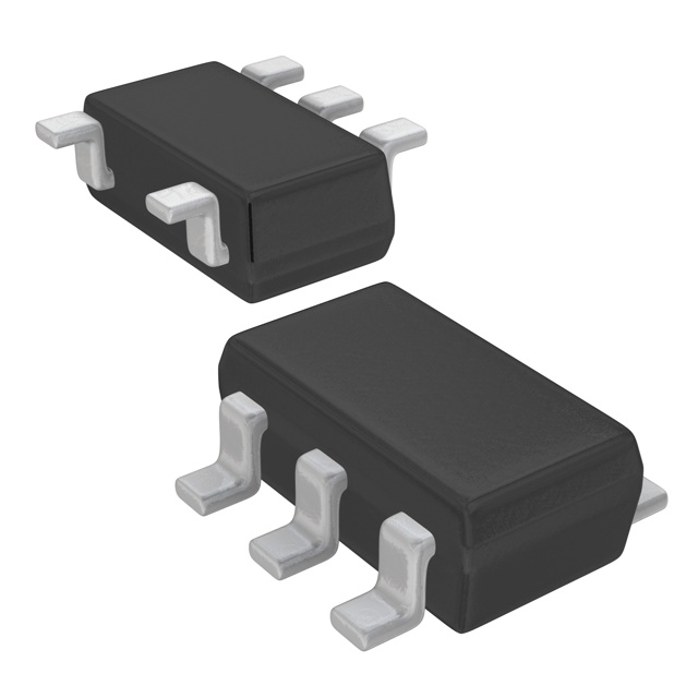
Package
XC6121F618MR-G comes in a small surface-mount package.
Essence
The essence of XC6121F618MR-G lies in its ability to provide stable voltage output for various electronic devices.
Packaging/Quantity
XC6121F618MR-G is typically packaged in reels and is available in large quantities.
Specifications
- Input Voltage Range: 2.5V - 6.0V
- Output Voltage: 1.8V
- Maximum Output Current: 150mA
- Dropout Voltage: 200mV (typical)
- Operating Temperature Range: -40°C to +85°C
Detailed Pin Configuration
XC6121F618MR-G has the following pin configuration:
- VIN (Input Voltage)
- GND (Ground)
- VOUT (Output Voltage)
Functional Features
- Voltage regulation within a specified range
- Overcurrent protection
- Thermal shutdown protection
- Low quiescent current
Advantages
- Small form factor allows for easy integration into compact electronic devices
- Efficient voltage regulation ensures stable performance of connected components
- Overcurrent and thermal shutdown protection enhance safety and reliability
Disadvantages
- Limited maximum output current may not be suitable for high-power applications
- Narrow input voltage range restricts compatibility with certain systems
Working Principles
XC6121F618MR-G utilizes internal circuitry to monitor and adjust the output voltage based on the input voltage and load conditions. It employs feedback mechanisms to maintain a stable output voltage within the specified range.
Detailed Application Field Plans
XC6121F618MR-G finds applications in various electronic devices, including but not limited to:
- Mobile phones
- Portable media players
- Digital cameras
- Wearable devices
- IoT devices
Detailed and Complete Alternative Models
Some alternative models that offer similar functionality to XC6121F618MR-G include:
- LM317
- LT1083
- LM7805
- LM1117
These models can be considered as alternatives based on specific requirements and compatibility with the target application.
In conclusion, XC6121F618MR-G is a voltage regulator that provides stable voltage output for electronic devices. Its compact size, low power consumption, and protective features make it suitable for a wide range of applications. However, its limitations in terms of maximum output current and input voltage range should be taken into consideration when selecting an appropriate model.
Seznam 10 běžných otázek a odpovědí souvisejících s aplikací XC6121F618MR-G v technických řešeních
Sure! Here are 10 common questions and answers related to the application of XC6121F618MR-G in technical solutions:
Q1: What is XC6121F618MR-G? A1: XC6121F618MR-G is a voltage detector IC (integrated circuit) manufactured by Torex Semiconductor. It is commonly used in various technical solutions for voltage monitoring and power management.
Q2: What is the operating voltage range of XC6121F618MR-G? A2: The operating voltage range of XC6121F618MR-G is from 0.6V to 6.0V.
Q3: What is the output type of XC6121F618MR-G? A3: XC6121F618MR-G has an open-drain output type.
Q4: What is the typical quiescent current consumption of XC6121F618MR-G? A4: The typical quiescent current consumption of XC6121F618MR-G is 1.0µA.
Q5: What is the purpose of the built-in delay circuit in XC6121F618MR-G? A5: The built-in delay circuit in XC6121F618MR-G provides a delay time to prevent false detection caused by momentary voltage fluctuations or noise.
Q6: Can XC6121F618MR-G be used for overvoltage protection? A6: No, XC6121F618MR-G is not designed for overvoltage protection. It is primarily used for undervoltage detection.
Q7: What is the maximum reset output current of XC6121F618MR-G? A7: The maximum reset output current of XC6121F618MR-G is 100mA.
Q8: Is XC6121F618MR-G suitable for battery-powered applications? A8: Yes, XC6121F618MR-G is suitable for battery-powered applications due to its low quiescent current consumption.
Q9: Can XC6121F618MR-G be used in automotive applications? A9: Yes, XC6121F618MR-G is AEC-Q100 qualified and can be used in automotive applications.
Q10: What is the package type of XC6121F618MR-G? A10: XC6121F618MR-G is available in a small SOT-25 package.

