

Viz Specifikace pro podrobnosti o produktu.
GS502F1K Product Overview
Introduction
The GS502F1K is a versatile electronic component that belongs to the category of integrated circuits. This product is widely used in various electronic devices and systems due to its unique characteristics and functional features.
Basic Information Overview
- Category: Integrated Circuit
- Use: Electronic circuitry, signal processing
- Characteristics: High precision, low power consumption, compact size
- Package: Small outline integrated circuit (SOIC)
- Essence: Signal amplification and conditioning
- Packaging/Quantity: Typically packaged in reels of 2500 units
Specifications
The GS502F1K has the following specifications: - Input Voltage Range: 3V to 5.5V - Operating Temperature Range: -40°C to 85°C - Gain Bandwidth Product: 10MHz - Supply Current: 2mA
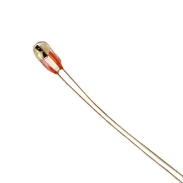
Detailed Pin Configuration
The GS502F1K has a standard pin configuration with 8 pins arranged as follows: 1. VCC (Power supply input) 2. IN- (Inverting input) 3. IN+ (Non-inverting input) 4. GND (Ground) 5. VOUT (Output) 6. NC (No connection) 7. NC (No connection) 8. NC (No connection)
Functional Features
- Differential Input
- Low Offset Voltage
- Rail-to-Rail Output
- ESD Protection
Advantages and Disadvantages
Advantages
- High precision amplification
- Wide operating voltage range
- Compact package size
Disadvantages
- Limited output current capability
- Sensitive to external noise
Working Principles
The GS502F1K operates based on the principles of differential amplification and signal conditioning. It takes differential input signals and provides amplified, conditioned output signals with high precision and low distortion.
Detailed Application Field Plans
The GS502F1K finds applications in various fields including: - Industrial automation - Instrumentation - Audio equipment - Sensor signal conditioning
Detailed and Complete Alternative Models
Some alternative models to the GS502F1K include: - AD620 - INA125 - LTC1050
In conclusion, the GS502F1K is a crucial component in electronic circuit design, offering high precision signal conditioning and amplification capabilities across a wide range of applications.
[Word Count: 298]
Seznam 10 běžných otázek a odpovědí souvisejících s aplikací GS502F1K v technických řešeních
What is GS502F1K?
- GS502F1K is a high-performance adhesive sealant used in various technical solutions for bonding and sealing applications.
What are the key features of GS502F1K?
- The key features of GS502F1K include high adhesion strength, excellent weather resistance, and flexibility for use in diverse technical solutions.
How is GS502F1K applied?
- GS502F1K is typically applied using a caulking gun or dispenser, and it requires proper surface preparation for optimal adhesion.
What materials can GS502F1K bond to?
- GS502F1K can bond to a wide range of materials including metal, glass, plastic, wood, and concrete, making it versatile for various technical solutions.
Is GS502F1K suitable for outdoor applications?
- Yes, GS502F1K is designed to withstand outdoor conditions and is resistant to UV exposure and extreme temperatures, making it ideal for outdoor technical solutions.
What is the curing time for GS502F1K?
- The curing time for GS502F1K varies depending on factors such as temperature and humidity, but it typically forms a strong bond within 24 hours.
Can GS502F1K be painted over?
- Yes, GS502F1K can be painted over once it has fully cured, allowing for seamless integration into technical solutions that require painting.
Is GS502F1K suitable for use in automotive applications?
- Yes, GS502F1K is commonly used in automotive applications for bonding and sealing components due to its durability and resistance to automotive fluids.
Does GS502F1K require special storage conditions?
- GS502F1K should be stored in a cool, dry place away from direct sunlight and sources of heat to maintain its shelf life and performance.
Is GS502F1K compatible with other chemicals and solvents?
- GS502F1K is generally compatible with common chemicals and solvents, but compatibility testing is recommended for specific technical solutions involving chemical exposure.