

Viz Specifikace pro podrobnosti o produktu.
SI7119DN-T1-E3
Product Overview
Category
The SI7119DN-T1-E3 belongs to the category of power management integrated circuits (PMICs).
Use
It is used for voltage regulation and power management in various electronic devices and systems.
Characteristics
- Voltage Regulation: Provides stable voltage output.
- Efficiency: High efficiency in converting and managing power.
- Compact Package: Small form factor for space-constrained applications.
- Reliability: Designed for reliable performance in diverse operating conditions.
Package
The SI7119DN-T1-E3 is available in a compact and durable package suitable for surface mount technology (SMT) assembly.
Essence
The essence of SI7119DN-T1-E3 lies in its ability to efficiently regulate and manage power supply, ensuring stable and reliable operation of electronic devices.
Packaging/Quantity
The SI7119DN-T1-E3 is typically supplied in reels containing a specific quantity based on customer requirements.
Specifications
- Input Voltage Range: 4.5V to 60V
- Output Voltage Range: 0.8V to 24V
- Maximum Output Current: 3A
- Operating Temperature Range: -40°C to 125°C
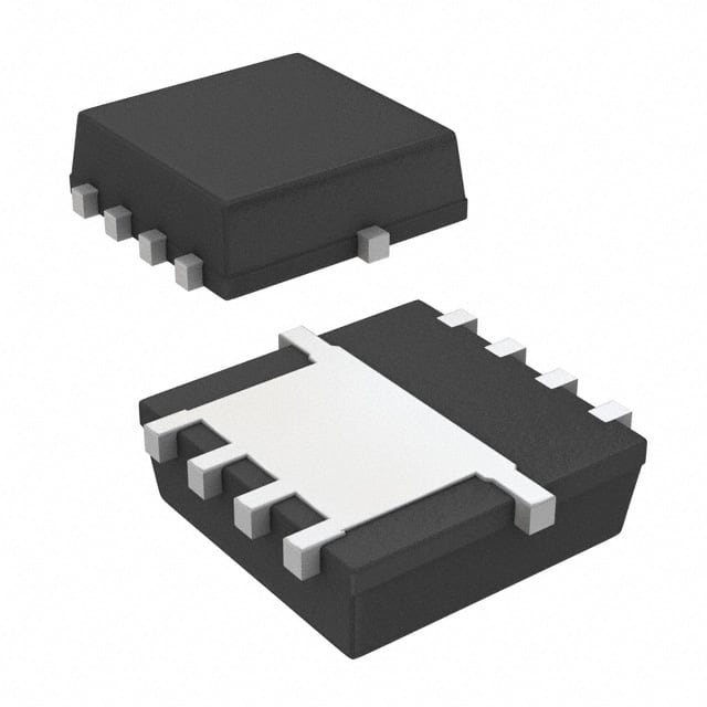
- Package Type: DFN-10 (3x3)
Detailed Pin Configuration
The SI7119DN-T1-E3 features a DFN-10 package with the following pin configuration: 1. VIN (Input Voltage) 2. GND (Ground) 3. EN (Enable) 4. FB (Feedback) 5. SS (Soft Start) 6. COMP (Compensation) 7. PGND (Power Ground) 8. SW (Switch Node) 9. BST (Bootstrap) 10. VOUT (Output Voltage)
Functional Features
- Wide Input Voltage Range: Allows operation from various power sources.
- Integrated Protection: Overcurrent, overvoltage, and thermal protection.
- Soft Start Function: Prevents inrush current during startup.
- Adjustable Output Voltage: Flexibility in setting the desired output voltage level.
Advantages and Disadvantages
Advantages
- High efficiency power management
- Wide input voltage range
- Integrated protection features
- Compact package size
Disadvantages
- Limited maximum output current compared to some alternatives
- May require external components for specific applications
Working Principles
The SI7119DN-T1-E3 operates by regulating the input voltage to provide a stable and controlled output voltage. It utilizes internal control circuitry and feedback mechanisms to achieve efficient power management while ensuring protection against fault conditions.
Detailed Application Field Plans
The SI7119DN-T1-E3 is well-suited for a wide range of applications including: - Industrial automation systems - Automotive electronics - Telecommunications equipment - Renewable energy systems - Consumer electronics
Detailed and Complete Alternative Models
Some alternative models to SI7119DN-T1-E3 include: - LM2675-ADJ - LT1763-3.3 - TPS5430DDAR - ADP2384ACPZ
These alternatives offer similar functionality and may be considered based on specific application requirements.
In conclusion, the SI7119DN-T1-E3 is a versatile power management IC with a wide range of applications and features that make it an essential component in modern electronic systems.
Word count: 512
Seznam 10 běžných otázek a odpovědí souvisejících s aplikací SI7119DN-T1-E3 v technických řešeních
What is the SI7119DN-T1-E3?
- The SI7119DN-T1-E3 is a dual N-channel 30 V (D-S) MOSFET in a small, thermally enhanced PowerPAK® SC-70 package.
What are the typical applications of the SI7119DN-T1-E3?
- It is commonly used in power management, load switching, and battery protection applications.
What is the maximum voltage rating for the SI7119DN-T1-E3?
- The maximum voltage rating for the SI7119DN-T1-E3 is 30 volts.
What is the maximum continuous drain current for the SI7119DN-T1-E3?
- The maximum continuous drain current for the SI7119DN-T1-E3 is 2.5 amperes.
What is the on-resistance of the SI7119DN-T1-E3?
- The on-resistance of the SI7119DN-T1-E3 is typically 60 milliohms at a VGS of 10 volts.
What is the thermal resistance of the SI7119DN-T1-E3?
- The thermal resistance of the SI7119DN-T1-E3 is typically 125°C/W.
Is the SI7119DN-T1-E3 suitable for use in battery protection circuits?
- Yes, the SI7119DN-T1-E3 is suitable for use in battery protection circuits due to its low on-resistance and high current handling capability.
Can the SI7119DN-T1-E3 be used in load switching applications?
- Yes, the SI7119DN-T1-E3 is well-suited for load switching applications due to its low on-resistance and high current rating.
Does the SI7119DN-T1-E3 require external heat sinking?
- In most applications, the SI7119DN-T1-E3 does not require external heat sinking due to its thermally enhanced PowerPAK® SC-70 package.
Are there any recommended layout considerations for using the SI7119DN-T1-E3 in a technical solution?
- Yes, it is recommended to minimize the length and width of the PCB traces connected to the SI7119DN-T1-E3 to reduce parasitic resistance and inductance. Additionally, proper attention should be given to thermal management to ensure optimal performance.