

Viz Specifikace pro podrobnosti o produktu.
SQJ488EP-T1_GE3
Product Overview
Category: Semiconductor
Use: Power MOSFET
Characteristics: High voltage, high current
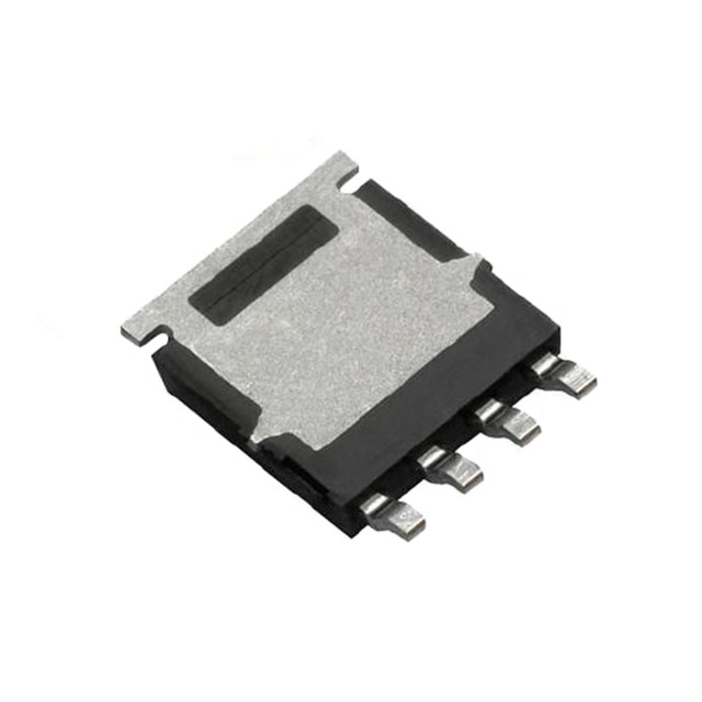
Package: TO-263-3
Essence: Efficient power switching
Packaging/Quantity: Tape and reel, 2500 units
Specifications
- Voltage Rating: 150V
- Current Rating: 80A
- RDS(ON): 4.8mΩ
- Gate Charge (Qg): 60nC
- Operating Temperature Range: -55°C to 175°C
Detailed Pin Configuration
- Source
- Gate
- Drain
Functional Features
- Low on-resistance
- Fast switching speed
- Low gate charge
- Avalanche energy rated
Advantages
- High efficiency
- Reduced power dissipation
- Enhanced system reliability
- Suitable for high frequency applications
Disadvantages
- Sensitive to overvoltage spikes
- Requires careful handling during installation
Working Principles
The SQJ488EP-T1_GE3 operates by controlling the flow of current between the source and drain terminals using the gate voltage. When a suitable voltage is applied to the gate, the MOSFET allows current to flow through, acting as a switch.
Detailed Application Field Plans
This MOSFET is commonly used in power supplies, motor control, and automotive applications due to its high voltage and current capabilities. It is also suitable for use in DC-DC converters and battery management systems.
Detailed and Complete Alternative Models
- IRF1405PBF
- FDP8870
Note: The alternative models listed above are provided for reference and may have different specifications.
This information provides a comprehensive overview of the SQJ488EP-T1_GE3, including its category, use, characteristics, package details, specifications, pin configuration, functional features, advantages and disadvantages, working principles, application field plans, and alternative models.
Seznam 10 běžných otázek a odpovědí souvisejících s aplikací SQJ488EP-T1_GE3 v technických řešeních
What is SQJ488EP-T1_GE3?
- SQJ488EP-T1_GE3 is a high-speed switching diode designed for use in various technical solutions such as signal processing, power management, and RF applications.
What are the key features of SQJ488EP-T1_GE3?
- The key features of SQJ488EP-T1_GE3 include low forward voltage, high reverse voltage, fast switching speed, and low capacitance.
In what applications can SQJ488EP-T1_GE3 be used?
- SQJ488EP-T1_GE3 can be used in applications such as rectification, signal demodulation, signal mixing, and high-frequency switching.
What is the maximum forward voltage of SQJ488EP-T1_GE3?
- The maximum forward voltage of SQJ488EP-T1_GE3 is typically around 0.7V at a forward current of 10mA.
What is the reverse recovery time of SQJ488EP-T1_GE3?
- The reverse recovery time of SQJ488EP-T1_GE3 is typically in the range of nanoseconds, making it suitable for high-speed switching applications.
Can SQJ488EP-T1_GE3 be used in power supply designs?
- Yes, SQJ488EP-T1_GE3 can be used in power supply designs for rectification and voltage regulation due to its low forward voltage and high reverse voltage capabilities.
Does SQJ488EP-T1_GE3 have any temperature limitations?
- SQJ488EP-T1_GE3 has a wide operating temperature range, typically from -55°C to 150°C, making it suitable for various environmental conditions.
What are the packaging options available for SQJ488EP-T1_GE3?
- SQJ488EP-T1_GE3 is available in various surface mount packages such as SOD-323 and SOD-523, providing flexibility for different PCB layouts.
Is SQJ488EP-T1_GE3 RoHS compliant?
- Yes, SQJ488EP-T1_GE3 is RoHS compliant, ensuring that it meets environmental regulations and standards.
Where can I find detailed specifications and application notes for SQJ488EP-T1_GE3?
- Detailed specifications and application notes for SQJ488EP-T1_GE3 can be found in the product datasheet provided by the manufacturer or distributor.