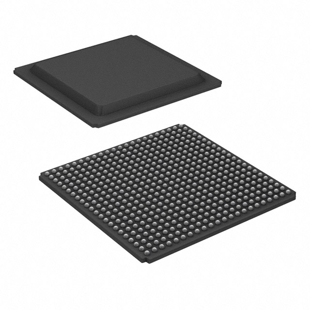
Viz Specifikace pro podrobnosti o produktu.

XA7S50-1FGGA484I
Product Overview
Category
The XA7S50-1FGGA484I belongs to the category of Field Programmable Gate Arrays (FPGAs).
Use
FPGAs are integrated circuits that can be programmed and reprogrammed to perform various digital functions. The XA7S50-1FGGA484I is specifically designed for applications requiring high-performance processing and programmable logic capabilities.
Characteristics
- High-performance FPGA with advanced programmable logic resources.
- Offers a wide range of I/O interfaces and connectivity options.
- Provides flexible and customizable solutions for complex digital designs.
- Supports rapid prototyping and development of electronic systems.
Package
The XA7S50-1FGGA484I comes in a compact and durable package, ensuring protection during handling and installation.
Essence
The essence of the XA7S50-1FGGA484I lies in its ability to provide a versatile platform for implementing complex digital designs and algorithms.
Packaging/Quantity
The XA7S50-1FGGA484I is typically packaged individually and is available in single-unit quantities.
Specifications
- FPGA Family: Xilinx 7 Series
- Device Type: Spartan-7
- Logic Cells: 52,160
- Flip-Flops: 104,320
- Block RAM: 2,700 Kbits
- DSP Slices: 240
- Clock Management Tiles: 4
- Maximum Operating Frequency: Up to 450 MHz
- I/O Voltage Levels: 3.3V
- Package Type: FGGA484
- Package Pins: 484
Detailed Pin Configuration
For a detailed pin configuration diagram of the XA7S50-1FGGA484I, please refer to the manufacturer's datasheet or documentation.
Functional Features
- High-performance programmable logic resources for complex digital designs.
- Flexible I/O interfaces for seamless integration with external devices.
- Advanced clock management capabilities for precise timing control.
- On-chip memory blocks for efficient data storage and retrieval.
- Dedicated DSP slices for implementing signal processing algorithms.
Advantages and Disadvantages
Advantages
- Versatile and customizable platform for digital design implementation.
- High-performance processing capabilities.
- Rapid prototyping and development of electronic systems.
- Extensive connectivity options for seamless integration.
Disadvantages
- Steeper learning curve compared to traditional fixed-function integrated circuits.
- Higher power consumption compared to dedicated application-specific integrated circuits (ASICs).
- Relatively higher cost compared to simpler programmable logic devices.
Working Principles
The XA7S50-1FGGA484I operates based on the principles of field-programmable gate arrays. It consists of a matrix of configurable logic blocks interconnected through programmable routing resources. The device can be programmed using hardware description languages (HDL) or specialized design software, allowing users to define the desired functionality and interconnections of the FPGA.
Once programmed, the XA7S50-1FGGA484I executes the specified digital functions by routing signals through the configured logic blocks and interconnects. This enables the FPGA to perform complex computations, data processing, and control tasks as per the user's requirements.
Detailed Application Field Plans
The XA7S50-1FGGA484I finds applications in various fields, including but not limited to:
- Communications: Used in wireless base stations, network routers, and communication infrastructure equipment.
- Industrial Automation: Employed in control systems, robotics, and factory automation.
- Aerospace and Defense: Utilized in radar systems, avionics, and military-grade electronics.
- Medical Devices: Integrated into medical imaging equipment, patient monitoring systems, and diagnostic devices.
- Automotive: Applied in advanced driver-assistance systems (ADAS), infotainment systems, and engine control units.
Detailed and Complete Alternative Models
- XA7S25-1FGGA484I: A lower-capacity variant of the XA7S50-1FGGA484I with 25,600 logic cells.
- XA7S100-1FGGA484I: A higher-capacity variant of the XA7S50-1FGGA484I with 100,352 logic cells.
- XA7S200-1FGGA484I: An even higher-capacity variant of the XA7S50-1FGGA484I with 200,704 logic cells.
These alternative models provide options for different project requirements, allowing users to choose the FPGA that best suits their specific needs.
Word count: 552 words
Seznam 10 běžných otázek a odpovědí souvisejících s aplikací XA7S50-1FGGA484I v technických řešeních
Sure! Here are 10 common questions and answers related to the application of XA7S50-1FGGA484I in technical solutions:
1. What is XA7S50-1FGGA484I? - XA7S50-1FGGA484I is a specific model of Field-Programmable Gate Array (FPGA) manufactured by Xilinx.
2. What is an FPGA? - FPGA stands for Field-Programmable Gate Array. It is a type of integrated circuit that can be programmed after manufacturing to perform specific functions.
3. What are the key features of XA7S50-1FGGA484I? - Some key features of XA7S50-1FGGA484I include 50,000 logic cells, 1,620 Kb block RAM, 4 PLLs, and 100+ I/O pins.
4. What are the typical applications of XA7S50-1FGGA484I? - XA7S50-1FGGA484I is commonly used in various technical solutions such as digital signal processing, embedded systems, robotics, aerospace, telecommunications, and high-performance computing.
5. How can XA7S50-1FGGA484I be programmed? - XA7S50-1FGGA484I can be programmed using Hardware Description Languages (HDLs) like VHDL or Verilog, which describe the desired functionality of the FPGA.
6. Can XA7S50-1FGGA484I be reprogrammed? - Yes, XA7S50-1FGGA484I is a reprogrammable FPGA, allowing users to modify its functionality by reprogramming it with new designs.
7. What development tools are available for programming XA7S50-1FGGA484I? - Xilinx provides various development tools like Vivado Design Suite, which includes a graphical interface and compiler for designing and programming FPGAs.
8. What is the power consumption of XA7S50-1FGGA484I? - The power consumption of XA7S50-1FGGA484I depends on the specific design and usage scenario. It is recommended to refer to the datasheet or consult Xilinx for detailed power consumption information.
9. Can XA7S50-1FGGA484I interface with other components or devices? - Yes, XA7S50-1FGGA484I can interface with various components and devices through its I/O pins, allowing communication with sensors, actuators, memory modules, and other peripherals.
10. Are there any limitations or considerations when using XA7S50-1FGGA484I? - Some considerations include understanding the FPGA's capabilities, ensuring proper power supply and cooling, managing I/O constraints, and optimizing the design for performance and resource utilization.
Please note that the answers provided here are general and may vary depending on the specific requirements and use cases.

