

Viz Specifikace pro podrobnosti o produktu.
XC2S100E-6PQG208C
Product Overview
Category
XC2S100E-6PQG208C belongs to the category of programmable logic devices (PLDs).
Use
This product is widely used in various electronic applications that require high-speed digital signal processing and complex logic functions.
Characteristics
- High-performance programmable logic device
- Offers a large number of configurable logic blocks (CLBs) and input/output blocks (IOBs)
- Provides flexible interconnect resources for implementing complex digital designs
- Supports advanced features such as embedded memory blocks and digital clock managers
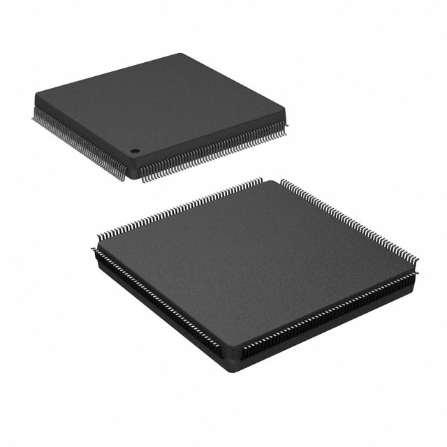
Package
XC2S100E-6PQG208C is available in a PQG208 package, which refers to a plastic quad flat pack with 208 pins.
Essence
The essence of XC2S100E-6PQG208C lies in its ability to provide a versatile platform for designing and implementing complex digital circuits.
Packaging/Quantity
This product is typically packaged in reels or trays, and the quantity per package depends on the manufacturer's specifications.
Specifications
- Device Type: Field Programmable Gate Array (FPGA)
- Logic Cells: 100,000
- Number of I/Os: 208
- Operating Voltage: 3.3V
- Speed Grade: -6 (indicating a maximum operating frequency of 6ns)
Detailed Pin Configuration
The pin configuration of XC2S100E-6PQG208C is as follows:
- VCCO
- GND
- IOL1P0
- IOL1N0
- IOL2P0
- IOL2N0
- IOL3P0
- IOL3N0
- IOL4P0
- IOL4N0
- IOL5P0
- IOL5N0 ... (continued for all 208 pins)
Functional Features
XC2S100E-6PQG208C offers the following functional features:
- Configurable Logic Blocks (CLBs): These blocks can be programmed to implement various logic functions, allowing for flexible design customization.
- Input/Output Blocks (IOBs): These blocks provide the interface between the FPGA and external devices, enabling data exchange.
- Embedded Memory Blocks: The device includes dedicated memory blocks that can be used for storing data or implementing lookup tables.
- Digital Clock Managers: XC2S100E-6PQG208C supports advanced clock management features, allowing precise control over timing requirements.
Advantages and Disadvantages
Advantages
- High-performance FPGA with a large number of logic cells
- Versatile and flexible design capabilities
- Supports advanced features such as embedded memory and clock management
- Suitable for complex digital designs requiring high-speed processing
Disadvantages
- Relatively higher power consumption compared to simpler programmable logic devices
- Steeper learning curve for beginners due to its complexity
Working Principles
XC2S100E-6PQG208C operates based on the principles of reconfigurable logic. It consists of configurable logic blocks (CLBs) interconnected through programmable routing resources. The device can be programmed using hardware description languages (HDLs) or graphical tools to define the desired functionality. Once programmed, the FPGA executes the configured logic operations.
Detailed Application Field Plans
XC2S100E-6PQG208C finds applications in various fields, including: 1. Telecommunications: Used in network routers, switches, and communication equipment for high-speed data processing. 2. Industrial Automation: Employed in control systems, robotics, and machine vision applications for real-time processing and control. 3. Aerospace and Defense: Utilized in radar systems, avionics, and military communication equipment for high-performance signal processing. 4. Medical Devices: Integrated into medical imaging systems, patient monitoring devices, and diagnostic equipment for data processing and analysis.
Detailed and Complete Alternative Models
Some alternative models to XC2S100E-6PQG208C include: 1. XC2S50E-6PQG208C: A lower-capacity version of the same FPGA family, suitable for smaller-scale designs. 2. XC2S200E-6PQG208C: A higher-capacity variant with double the logic cells, offering more design flexibility. 3. XC2S300E-6PQG208C: An even higher-capacity option, ideal for complex digital designs requiring extensive logic resources.
These alternative models provide varying levels of capacity and performance to cater to different design requirements.
In conclusion, XC2S100E-6PQG208C is a high-performance programmable logic device
Seznam 10 běžných otázek a odpovědí souvisejících s aplikací XC2S100E-6PQG208C v technických řešeních
Sure! Here are 10 common questions and answers related to the application of XC2S100E-6PQG208C in technical solutions:
Question: What is XC2S100E-6PQG208C?
- Answer: XC2S100E-6PQG208C is a specific model of Xilinx Spartan-II FPGA (Field-Programmable Gate Array) with 100,000 system gates.Question: What are the key features of XC2S100E-6PQG208C?
- Answer: Some key features include 100,000 system gates, 208-pin PQFP package, 6ns maximum pin-to-pin delay, and 3.3V power supply.Question: What are the typical applications of XC2S100E-6PQG208C?
- Answer: XC2S100E-6PQG208C is commonly used in various technical solutions such as digital signal processing, embedded systems, communication systems, and industrial automation.Question: How can XC2S100E-6PQG208C be programmed?
- Answer: XC2S100E-6PQG208C can be programmed using Xilinx's programming tools like iMPACT or Vivado, which allow users to configure the FPGA with their desired logic design.Question: What is the maximum operating frequency of XC2S100E-6PQG208C?
- Answer: The maximum operating frequency of XC2S100E-6PQG208C depends on the complexity of the design and implementation, but it can typically reach frequencies in the range of tens to hundreds of megahertz.Question: Can XC2S100E-6PQG208C interface with other components or devices?
- Answer: Yes, XC2S100E-6PQG208C can interface with various components and devices through its I/O pins, which support different voltage standards and protocols such as LVCMOS, LVTTL, and LVDS.Question: Is XC2S100E-6PQG208C suitable for low-power applications?
- Answer: While XC2S100E-6PQG208C is not specifically designed for low-power applications, it does offer power-saving features like clock gating and dynamic power management that can be utilized to optimize power consumption.Question: Can XC2S100E-6PQG208C be reprogrammed multiple times?
- Answer: Yes, XC2S100E-6PQG208C is a reprogrammable FPGA, allowing users to reconfigure it multiple times with different designs or updates as needed.Question: Are there any development boards available for XC2S100E-6PQG208C?
- Answer: Yes, Xilinx provides development boards like the Spartan-II Starter Kit that are compatible with XC2S100E-6PQG208C, enabling users to prototype and test their designs.Question: Where can I find more information about XC2S100E-6PQG208C?
- Answer: You can find more detailed information about XC2S100E-6PQG208C in the official Xilinx documentation, including datasheets, user guides, and application notes available on their website.