

Viz Specifikace pro podrobnosti o produktu.
XC2V1000-4FF896I
Product Overview
Category
The XC2V1000-4FF896I belongs to the category of Field Programmable Gate Arrays (FPGAs).
Use
FPGAs are integrated circuits that can be programmed and reprogrammed to perform various digital functions. The XC2V1000-4FF896I is specifically designed for high-performance applications requiring complex logic functions.
Characteristics
- High-density programmable logic device
- Advanced architecture for efficient performance
- Flexible and customizable design options
- Fast processing speed
- Low power consumption
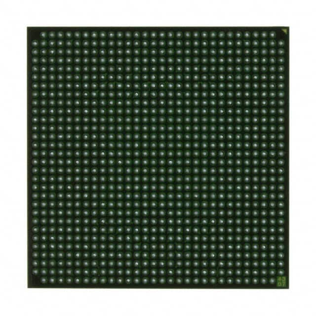
Package
The XC2V1000-4FF896I comes in a Fine-Pitch Ball Grid Array (FBGA) package.
Essence
The essence of the XC2V1000-4FF896I lies in its ability to provide a versatile and powerful platform for implementing complex digital designs.
Packaging/Quantity
The XC2V1000-4FF896I is typically packaged individually and is available in varying quantities depending on the manufacturer's specifications.
Specifications
- Device Type: FPGA
- Logic Cells: 1,000
- Maximum Frequency: 200 MHz
- Number of I/Os: 896
- Operating Voltage: 3.3V
- Package Type: FBGA
- Package Pins: 896
- Temperature Range: -40°C to +85°C
Detailed Pin Configuration
The XC2V1000-4FF896I has a total of 896 pins, which are assigned to various functions such as input/output, power supply, configuration, and clock signals. A detailed pin configuration diagram can be found in the product datasheet provided by the manufacturer.
Functional Features
- High-speed data processing capabilities
- Configurable logic blocks for flexible design implementation
- Dedicated memory resources for efficient storage and retrieval
- Built-in arithmetic functions for mathematical operations
- Support for various communication protocols
- On-chip configuration memory for easy reprogramming
Advantages and Disadvantages
Advantages
- Versatile and customizable design options
- High-performance capabilities
- Fast processing speed
- Low power consumption compared to alternative solutions
- Easy reprogramming for iterative design improvements
Disadvantages
- Higher cost compared to traditional fixed-function integrated circuits
- Steeper learning curve for programming and utilizing the full potential of FPGAs
- Limited availability of specialized technical support compared to mainstream technologies
Working Principles
The XC2V1000-4FF896I operates based on the principles of configurable logic. It consists of an array of programmable logic cells interconnected through a network of configurable routing resources. The logic cells can be programmed to implement desired digital functions, and the interconnections can be configured to establish desired signal paths. This flexibility allows the FPGA to adapt to various application requirements.
Detailed Application Field Plans
The XC2V1000-4FF896I finds applications in a wide range of fields, including but not limited to: - Telecommunications - Aerospace and defense - Industrial automation - Medical devices - Automotive electronics - Consumer electronics
In telecommunications, the XC2V1000-4FF896I can be used for high-speed data processing, protocol conversion, and signal conditioning. In aerospace and defense, it can be utilized for radar signal processing, image recognition, and encryption algorithms. In industrial automation, it can enable complex control systems and real-time monitoring. In medical devices, it can facilitate advanced imaging and diagnostics. In automotive electronics, it can support driver assistance systems and infotainment. In consumer electronics, it can enhance multimedia processing and gaming experiences.
Detailed and Complete Alternative Models
Some alternative models to the XC2V1000-4FF896I that offer similar functionality and performance include: - Altera Cyclone IV EP4CE115F29C7 - Xilinx Spartan-6 XC6SLX9-2CSG324C - Lattice Semiconductor iCE40HX1K-TQ144
These alternative models provide a range of options with varying capacities, features, and price points to suit different application requirements.
In conclusion, the XC2V1000-4FF896I is a high-density FPGA with advanced architecture, offering flexibility, high-performance capabilities, and low power consumption. Its versatile nature makes it suitable for various applications across multiple industries. While it has advantages such as customizable design options and fast processing speed, it also has disadvantages like higher cost and a steeper learning curve. Nonetheless, the XC2V1000-4FF896I remains a powerful tool for implementing complex digital designs in diverse fields.
Seznam 10 běžných otázek a odpovědí souvisejících s aplikací XC2V1000-4FF896I v technických řešeních
Sure! Here are 10 common questions and answers related to the application of XC2V1000-4FF896I in technical solutions:
Q: What is XC2V1000-4FF896I? A: XC2V1000-4FF896I is a field-programmable gate array (FPGA) manufactured by Xilinx, designed for high-performance digital applications.
Q: What are the key features of XC2V1000-4FF896I? A: Some key features include 1,000,000 system gates, 3.3V operation, 4ns pin-to-pin delay, 896-pin FineLine BGA package, and 4-input look-up tables (LUTs).
Q: What are the typical applications of XC2V1000-4FF896I? A: XC2V1000-4FF896I is commonly used in various technical solutions such as telecommunications, industrial automation, aerospace, defense systems, medical equipment, and image/video processing.
Q: How can XC2V1000-4FF896I be programmed? A: XC2V1000-4FF896I can be programmed using Xilinx's ISE Design Suite software, which allows users to design and implement their logic circuits onto the FPGA.
Q: Can XC2V1000-4FF896I be reprogrammed after deployment? A: Yes, XC2V1000-4FF896I is a reprogrammable FPGA, meaning it can be reconfigured with different designs even after it has been deployed in a system.
Q: What are the advantages of using XC2V1000-4FF896I in technical solutions? A: Some advantages include high flexibility, fast time-to-market, low power consumption, high-performance processing capabilities, and the ability to implement complex algorithms.
Q: Are there any limitations or considerations when using XC2V1000-4FF896I? A: Some considerations include limited I/O pins, potential power supply requirements, the need for expertise in FPGA design, and the possibility of increased development time compared to using off-the-shelf components.
Q: Can XC2V1000-4FF896I interface with other electronic components? A: Yes, XC2V1000-4FF896I can interface with various electronic components such as memory modules, sensors, communication interfaces, and other digital logic devices.
Q: Is XC2V1000-4FF896I suitable for real-time applications? A: Yes, XC2V1000-4FF896I is capable of handling real-time applications due to its high-speed processing capabilities and low-latency performance.
Q: Where can I find additional resources and support for XC2V1000-4FF896I? A: Xilinx provides comprehensive documentation, application notes, reference designs, and technical support through their website and online community forums.
Please note that the answers provided here are general and may vary depending on specific use cases and requirements.