

Viz Specifikace pro podrobnosti o produktu.
XC2VP40-6FF1152I
Product Overview
Category
XC2VP40-6FF1152I belongs to the category of Field Programmable Gate Arrays (FPGAs).
Use
This FPGA is primarily used in digital logic circuits for various applications such as telecommunications, automotive, aerospace, and consumer electronics.
Characteristics
- High-performance programmable logic device
- Offers a large number of configurable logic blocks
- Provides flexible interconnect resources
- Supports high-speed data processing
- Enables rapid prototyping and system development
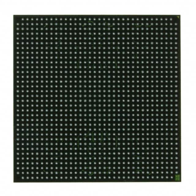
Package
XC2VP40-6FF1152I comes in a compact and durable package designed to withstand harsh operating conditions.
Essence
The essence of XC2VP40-6FF1152I lies in its ability to provide a versatile and customizable solution for complex digital circuit designs.
Packaging/Quantity
Each package of XC2VP40-6FF1152I contains one unit of the FPGA.
Specifications
- Model: XC2VP40-6FF1152I
- Logic Cells: 40,000
- Maximum Frequency: 500 MHz
- I/O Pins: 1,152
- Operating Voltage: 1.2V
- Package Type: FF1152
Detailed Pin Configuration
The detailed pin configuration of XC2VP40-6FF1152I can be found in the product datasheet provided by the manufacturer.
Functional Features
- High-speed data processing capabilities
- Configurable logic blocks for custom circuit implementation
- Flexible interconnect resources for efficient signal routing
- On-chip memory elements for data storage
- Support for various communication protocols
- Built-in security features for protecting intellectual property
Advantages and Disadvantages
Advantages
- Versatile and customizable solution for complex digital circuit designs
- Rapid prototyping and system development capabilities
- High-performance and high-speed data processing
- Support for various communication protocols
Disadvantages
- Steep learning curve for beginners due to the complexity of FPGA programming
- Relatively higher cost compared to other programmable logic devices
- Limited availability of technical support for specific design challenges
Working Principles
XC2VP40-6FF1152I operates based on the principles of reconfigurable digital logic. It consists of configurable logic blocks, interconnect resources, and memory elements. The FPGA can be programmed to implement complex digital circuits by configuring the logic blocks and routing signals through the interconnect resources.
Detailed Application Field Plans
XC2VP40-6FF1152I finds applications in various fields, including: 1. Telecommunications: Used in network routers, switches, and base stations. 2. Automotive: Employed in advanced driver-assistance systems (ADAS) and engine control units (ECUs). 3. Aerospace: Utilized in satellite communication systems and avionics. 4. Consumer Electronics: Integrated into high-definition televisions, gaming consoles, and multimedia devices.
Detailed and Complete Alternative Models
Some alternative models to XC2VP40-6FF1152I include: 1. XC2VP50-6FFG1152C 2. XC2VP100-6FF1704I 3. XC2VP200-6FF1704C 4. XC2VP400-6FF1704I
These models offer similar functionality but may vary in terms of logic capacity, I/O pins, and package type.
Word count: 496 words
Seznam 10 běžných otázek a odpovědí souvisejících s aplikací XC2VP40-6FF1152I v technických řešeních
What is the maximum operating frequency of XC2VP40-6FF1152I?
- The maximum operating frequency of XC2VP40-6FF1152I is 400 MHz.What are the typical applications for XC2VP40-6FF1152I?
- XC2VP40-6FF1152I is commonly used in high-performance computing, networking, and telecommunications applications.What is the power consumption of XC2VP40-6FF1152I?
- The power consumption of XC2VP40-6FF1152I varies depending on the operating conditions, but it typically ranges from 5W to 10W.Can XC2VP40-6FF1152I be used in industrial control systems?
- Yes, XC2VP40-6FF1152I is suitable for use in industrial control systems due to its reliability and performance.What are the available I/O standards for XC2VP40-6FF1152I?
- XC2VP40-6FF1152I supports various I/O standards including LVCMOS, LVTTL, HSTL, SSTL, and more.Is XC2VP40-6FF1152I compatible with common development tools?
- Yes, XC2VP40-6FF1152I is compatible with popular FPGA development tools such as Xilinx ISE and Vivado.What are the key features of XC2VP40-6FF1152I that make it suitable for high-speed data processing?
- XC2VP40-6FF1152I features high-speed transceivers, large internal memory, and advanced DSP capabilities for efficient data processing.Can XC2VP40-6FF1152I be used in space-constrained designs?
- Yes, XC2VP40-6FF1152I is available in a compact package and can be used in space-constrained designs.What are the temperature specifications for XC2VP40-6FF1152I?
- XC2VP40-6FF1152I has a wide operating temperature range, typically from -40°C to 100°C.Are there any known compatibility issues when using XC2VP40-6FF1152I with other components?
- XC2VP40-6FF1152I is designed to be compatible with a wide range of components, but it's important to refer to the datasheet and application notes for specific compatibility considerations.