

Viz Specifikace pro podrobnosti o produktu.
XC2VP70-6FF1517I
Product Overview
Category
XC2VP70-6FF1517I belongs to the category of Field Programmable Gate Arrays (FPGAs).
Use
This FPGA is designed for high-performance applications that require complex digital logic circuits. It offers flexibility and reconfigurability, making it suitable for a wide range of industries.
Characteristics
- High-performance FPGA with advanced features
- Reconfigurable architecture allows for customization
- Offers high-speed data processing capabilities
- Supports complex digital logic designs
- Provides flexibility in system integration
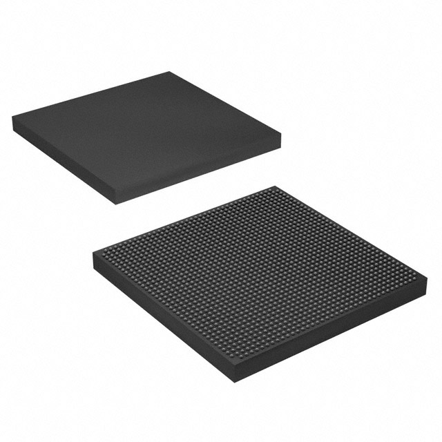
Package
XC2VP70-6FF1517I comes in a compact package that ensures easy installation and integration into electronic systems. The package is designed to protect the FPGA from external factors such as moisture and static electricity.
Essence
The essence of XC2VP70-6FF1517I lies in its ability to provide a customizable and high-performance solution for digital logic circuit implementation. It enables designers to create complex systems with ease.
Packaging/Quantity
XC2VP70-6FF1517I is typically packaged individually and is available in various quantities depending on the requirements of the user or project.
Specifications
- FPGA Family: Virtex-II Pro
- Logic Cells: 70,000
- System Gates: 1,500,000
- Number of I/Os: 680
- Operating Voltage: 1.5V
- Maximum Frequency: 400 MHz
- Package Type: FF1517
Detailed Pin Configuration
The detailed pin configuration of XC2VP70-6FF1517I can be found in the product datasheet provided by the manufacturer. It includes information about the input/output pins, power supply pins, and other necessary connections.
Functional Features
XC2VP70-6FF1517I offers several functional features that enhance its performance and usability:
High-Speed Data Processing: The FPGA supports high-speed data processing, making it suitable for applications that require real-time data handling.
Reconfigurability: The reconfigurable architecture allows users to modify the functionality of the FPGA even after deployment, providing flexibility in system design.
Integrated IP Cores: XC2VP70-6FF1517I incorporates various Intellectual Property (IP) cores, such as memory controllers and communication interfaces, which simplify system integration.
Advanced DSP Capabilities: The FPGA includes Digital Signal Processing (DSP) blocks that enable efficient implementation of complex algorithms, making it ideal for signal processing applications.
Advantages and Disadvantages
Advantages
- High-performance FPGA with advanced features
- Reconfigurable architecture allows for customization
- Supports complex digital logic designs
- Offers flexibility in system integration
- Integrated IP cores simplify system development
Disadvantages
- Relatively high power consumption compared to other programmable logic devices
- Steeper learning curve for beginners due to its complexity
Working Principles
XC2VP70-6FF1517I operates based on the principles of digital logic circuits. It consists of configurable logic blocks, interconnects, and input/output elements. The user can program the FPGA to implement desired logic functions by configuring the interconnections between logic blocks.
The FPGA's internal configuration memory stores the user-defined logic circuit, allowing for reconfiguration when needed. During operation, the FPGA processes incoming data according to the programmed logic, producing the desired output.
Detailed Application Field Plans
XC2VP70-6FF1517I finds applications in various fields, including:
- Telecommunications: Used in network routers, switches, and base stations for high-speed data processing and protocol handling.
- Aerospace and Defense: Employed in radar systems, avionics, and military communication systems for their high-performance and reconfigurable nature.
- Industrial Automation: Utilized in control systems, robotics, and machine vision applications for real-time data processing and control.
- Medical Devices: Integrated into medical imaging equipment, patient monitoring systems, and diagnostic devices to handle complex algorithms and data processing.
Detailed and Complete Alternative Models
- XC2VP30-6FF1517I: A lower-cost alternative with reduced logic capacity but similar features.
- XC2VP100-6FF1704C: A higher-capacity FPGA with increased logic cells and system gates for more demanding applications.
- XC2V8000-4FFG1152C: An ultra-high-capacity FPGA suitable for large-scale designs requiring extensive logic resources.
These alternative models offer varying levels of performance and capacity to cater to different project requirements.
Word count: 550 words
Seznam 10 běžných otázek a odpovědí souvisejících s aplikací XC2VP70-6FF1517I v technických řešeních
Sure! Here are 10 common questions and answers related to the application of XC2VP70-6FF1517I in technical solutions:
Question: What is XC2VP70-6FF1517I?
- Answer: XC2VP70-6FF1517I is a specific model of Field Programmable Gate Array (FPGA) manufactured by Xilinx.Question: What are the key features of XC2VP70-6FF1517I?
- Answer: Some key features of XC2VP70-6FF1517I include a high gate count, low power consumption, and support for various I/O standards.Question: In what technical solutions can XC2VP70-6FF1517I be used?
- Answer: XC2VP70-6FF1517I can be used in a wide range of applications such as telecommunications, aerospace, defense, industrial automation, and image processing.Question: What advantages does XC2VP70-6FF1517I offer over other FPGAs?
- Answer: XC2VP70-6FF1517I offers a large number of logic gates, high-speed performance, and flexibility due to its programmable nature.Question: Can XC2VP70-6FF1517I be used for real-time signal processing?
- Answer: Yes, XC2VP70-6FF1517I can be used for real-time signal processing tasks due to its high-speed capabilities and parallel processing architecture.Question: How can XC2VP70-6FF1517I be programmed?
- Answer: XC2VP70-6FF1517I can be programmed using Hardware Description Languages (HDLs) such as VHDL or Verilog, along with Xilinx's development tools like Vivado or ISE.Question: Can XC2VP70-6FF1517I be used in safety-critical applications?
- Answer: Yes, XC2VP70-6FF1517I can be used in safety-critical applications as long as proper design and verification processes are followed to ensure reliability.Question: What is the power consumption of XC2VP70-6FF1517I?
- Answer: The power consumption of XC2VP70-6FF1517I depends on the specific design and usage scenario, but it generally has low power consumption compared to other FPGAs.Question: Does XC2VP70-6FF1517I support high-speed serial communication protocols?
- Answer: Yes, XC2VP70-6FF1517I supports various high-speed serial communication protocols such as PCIe, Ethernet, and USB.Question: Are there any limitations or considerations when using XC2VP70-6FF1517I?
- Answer: Some considerations include the need for proper cooling due to its power consumption, careful planning of I/O requirements, and understanding the specific requirements of the target application.
Please note that these answers are general and may vary depending on the specific implementation and requirements of your technical solution.