

Viz Specifikace pro podrobnosti o produktu.
XC3S50-4VQG100C
Product Overview
Category
The XC3S50-4VQG100C belongs to the category of programmable logic devices (PLDs).
Use
This product is widely used in various electronic applications that require high-performance digital logic functions.
Characteristics
- Programmable: The XC3S50-4VQG100C can be programmed to perform specific logic functions according to the user's requirements.
- High Performance: It offers fast processing speeds and efficient utilization of resources.
- Versatile: This PLD can be used in a wide range of applications due to its flexibility.
- Low Power Consumption: The XC3S50-4VQG100C is designed to operate with minimal power consumption, making it suitable for battery-powered devices.
Package
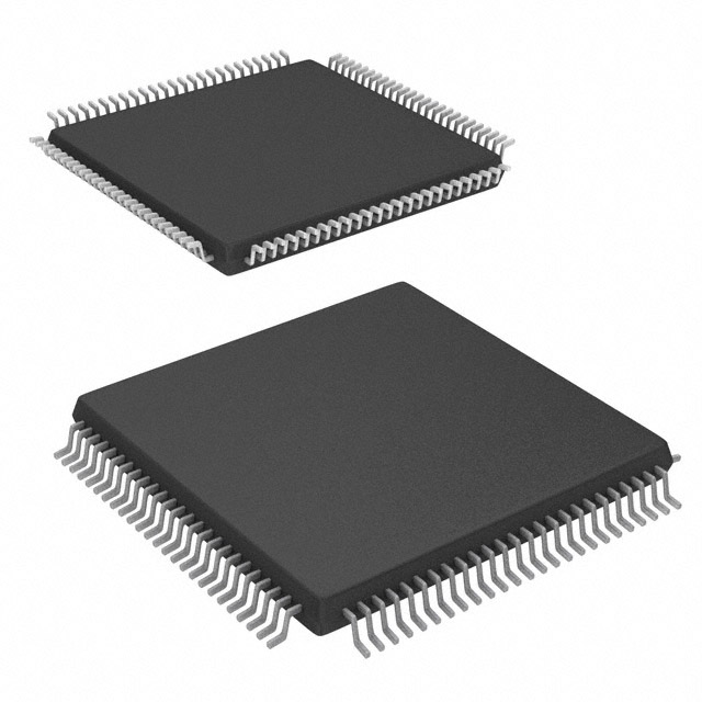
The XC3S50-4VQG100C comes in a Quad Flat No-Lead (QFN) package.
Essence
The essence of this product lies in its ability to provide customizable digital logic functions in a compact and energy-efficient package.
Packaging/Quantity
The XC3S50-4VQG100C is typically packaged in reels or trays, with a quantity of 100 units per package.
Specifications
- Device Type: Field-Programmable Gate Array (FPGA)
- Logic Cells: 50,000
- Operating Voltage: 1.2V
- Speed Grade: -4
- I/O Pins: 100
- Maximum Frequency: 300 MHz
- Configuration Memory: 4 Mb
- Package Type: QFN
- Temperature Range: -40°C to +85°C
Detailed Pin Configuration
The XC3S50-4VQG100C has a total of 100 I/O pins, which are configurable based on the desired functionality. These pins can be used for input, output, or bidirectional purposes, depending on the application requirements.
For a detailed pin configuration diagram, please refer to the datasheet provided by the manufacturer.
Functional Features
- High-Speed Processing: The XC3S50-4VQG100C offers fast processing capabilities, making it suitable for applications that require real-time data processing.
- Flexible I/O Configuration: The device allows for versatile I/O pin configuration, enabling seamless integration with other components and peripherals.
- On-Chip Memory: It includes embedded memory blocks that can be utilized for storing data or implementing complex algorithms.
- Built-in Clock Management: The XC3S50-4VQG100C features clock management resources, allowing precise control over timing requirements.
Advantages and Disadvantages
Advantages
- Customizable Logic Functions: The ability to program the XC3S50-4VQG100C according to specific requirements provides flexibility in design.
- Compact Size: The small form factor of this PLD makes it suitable for space-constrained applications.
- Low Power Consumption: The device operates efficiently with minimal power consumption, extending battery life in portable devices.
- High Performance: The XC3S50-4VQG100C offers fast processing speeds and efficient resource utilization.
Disadvantages
- Complexity: Programming and configuring the XC3S50-4VQG100C may require specialized knowledge and tools.
- Cost: Compared to traditional logic circuits, programmable logic devices like the XC3S50-4VQG100C can be more expensive.
Working Principles
The XC3S50-4VQG100C is based on the concept of field-programmable gate arrays (FPGAs). These devices consist of an array of configurable logic blocks interconnected through programmable interconnects. The user can program the FPGA to implement desired logic functions by configuring the interconnections and functionality of each logic block.
The XC3S50-4VQG100C utilizes a combination of look-up tables, flip-flops, and programmable interconnects to implement complex digital logic circuits. The configuration data is stored in on-chip memory and can be loaded during startup or reprogrammed as needed.
Detailed Application Field Plans
The XC3S50-4VQG100C finds applications in various fields, including:
- Communications: It can be used in networking equipment, routers, and switches for high-speed data processing and protocol handling.
- Industrial Automation: The device enables control and monitoring of industrial processes, such as robotics, machine vision, and motion control systems.
- Automotive Electronics: It can be utilized in automotive applications like engine control units (ECUs), advanced driver-assistance systems (ADAS), and infotainment systems.
- Consumer Electronics: The XC3S50-4VQG100C can be integrated into smart home devices, wearable technology, and multimedia systems.
- Aerospace and Defense: It finds applications in radar systems,
Seznam 10 běžných otázek a odpovědí souvisejících s aplikací XC3S50-4VQG100C v technických řešeních
Sure! Here are 10 common questions and answers related to the application of XC3S50-4VQG100C in technical solutions:
Question: What is XC3S50-4VQG100C?
Answer: XC3S50-4VQG100C is a specific model of Field-Programmable Gate Array (FPGA) manufactured by Xilinx.Question: What is an FPGA?
Answer: FPGA stands for Field-Programmable Gate Array, which is a type of integrated circuit that can be programmed after manufacturing to perform specific functions.Question: What are the key features of XC3S50-4VQG100C?
Answer: Some key features of XC3S50-4VQG100C include 50,000 logic cells, 4 input/output banks, and a VQG100C package.Question: What are the typical applications of XC3S50-4VQG100C?
Answer: XC3S50-4VQG100C is commonly used in various technical solutions such as digital signal processing, embedded systems, robotics, and telecommunications.Question: How can XC3S50-4VQG100C be programmed?
Answer: XC3S50-4VQG100C can be programmed using Hardware Description Languages (HDLs) like VHDL or Verilog, along with Xilinx's design software tools.Question: Can XC3S50-4VQG100C be reprogrammed multiple times?
Answer: Yes, XC3S50-4VQG100C is a reprogrammable FPGA, allowing users to modify its functionality multiple times.Question: What is the power supply requirement for XC3S50-4VQG100C?
Answer: XC3S50-4VQG100C typically requires a power supply voltage of 1.14V to 1.26V.Question: Does XC3S50-4VQG100C support external memory interfaces?
Answer: Yes, XC3S50-4VQG100C supports various external memory interfaces such as DDR, DDR2, and SDRAM.Question: Can XC3S50-4VQG100C communicate with other devices or microcontrollers?
Answer: Yes, XC3S50-4VQG100C can communicate with other devices or microcontrollers through various communication protocols like SPI, I2C, UART, or Ethernet.Question: Are there any development boards available for XC3S50-4VQG100C?
Answer: Yes, Xilinx provides development boards like the Spartan-3E Starter Kit that are compatible with XC3S50-4VQG100C, allowing users to prototype and test their designs.
Please note that the answers provided here are general and may vary depending on specific implementation requirements.