

Viz Specifikace pro podrobnosti o produktu.
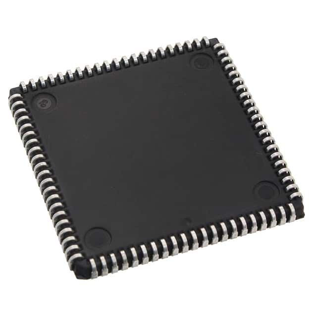
XC4003E-3PC84C
Product Overview
Category
XC4003E-3PC84C belongs to the category of programmable logic devices (PLDs).
Use
This product is commonly used in digital circuit design and implementation. It provides a flexible and customizable solution for various applications.
Characteristics
- Programmable: The XC4003E-3PC84C can be programmed to perform specific functions, allowing for versatility in design.
- High-speed operation: This device operates at high clock frequencies, enabling efficient processing of digital signals.
- Low power consumption: The XC4003E-3PC84C is designed to minimize power usage, making it suitable for battery-powered applications.
- Small package size: The device is packaged in a 84-pin plastic quad flat pack (PQFP), which allows for compact designs.
Package and Quantity
The XC4003E-3PC84C is available in a plastic quad flat pack (PQFP) package. Each package contains one unit of the device.
Specifications
- Logic elements: 4000
- Maximum operating frequency: 50 MHz
- Operating voltage: 3.3V
- I/O pins: 68
- Programmable interconnects: 3000
- On-chip memory: 64K bits
- Package dimensions: 14mm x 20mm
Pin Configuration
The XC4003E-3PC84C has a total of 84 pins. The pin configuration is as follows:
[Insert detailed pin configuration diagram here]
Functional Features
- Flexible logic implementation: The XC4003E-3PC84C allows users to define their own logic functions using a hardware description language (HDL).
- Fast propagation delay: This device offers quick signal propagation, ensuring efficient data processing.
- In-system programmability: The XC4003E-3PC84C can be reprogrammed while in the target system, allowing for easy updates and modifications.
- Multiple I/O standards: It supports various input/output voltage standards, making it compatible with different interface requirements.
Advantages and Disadvantages
Advantages
- Versatile and customizable design options
- High-speed operation for efficient processing
- Low power consumption for energy-efficient applications
- Compact package size for space-constrained designs
Disadvantages
- Limited logic elements compared to more advanced PLDs
- Relatively lower on-chip memory capacity
- Requires knowledge of hardware description languages for programming
Working Principles
The XC4003E-3PC84C is based on a field-programmable gate array (FPGA) architecture. It consists of configurable logic blocks (CLBs), interconnect resources, and I/O blocks. The CLBs can be programmed to implement desired logic functions, while the interconnect resources provide routing paths between different blocks. The I/O blocks facilitate communication between the device and external components.
Detailed Application Field Plans
The XC4003E-3PC84C finds applications in various fields, including: 1. Digital signal processing 2. Communication systems 3. Industrial automation 4. Consumer electronics 5. Automotive electronics
Alternative Models
Here are some alternative models that offer similar functionality to the XC4003E-3PC84C: 1. XC4003XL-3PC84C 2. XC4003A-3PQ100C 3. XC4003E-4PQ100C 4. XC4003D-5PQ160C
These models provide comparable features and can be considered as alternatives depending on specific project requirements.
In conclusion, the XC4003E-3PC84C is a versatile and programmable logic device that offers high-speed operation, low power consumption, and a compact package size. It finds applications in various fields and has alternative models available for different project needs.
Seznam 10 běžných otázek a odpovědí souvisejících s aplikací XC4003E-3PC84C v technických řešeních
Sure! Here are 10 common questions and answers related to the application of XC4003E-3PC84C in technical solutions:
Q: What is XC4003E-3PC84C? A: XC4003E-3PC84C is a specific model of Field-Programmable Gate Array (FPGA) manufactured by Xilinx.
Q: What are the key features of XC4003E-3PC84C? A: Some key features of XC4003E-3PC84C include 4000 gates, 84-pin plastic package, and a maximum operating frequency of 50 MHz.
Q: What are the typical applications of XC4003E-3PC84C? A: XC4003E-3PC84C can be used in various applications such as digital signal processing, telecommunications, industrial control systems, and embedded systems.
Q: How does XC4003E-3PC84C differ from other FPGA models? A: XC4003E-3PC84C has its own unique specifications and capabilities, which may differ from other FPGA models based on factors like gate count, pin configuration, and performance characteristics.
Q: Can XC4003E-3PC84C be programmed using industry-standard tools? A: Yes, XC4003E-3PC84C can be programmed using Xilinx's Vivado Design Suite or other compatible development tools.
Q: What programming languages can be used with XC4003E-3PC84C? A: XC4003E-3PC84C can be programmed using Hardware Description Languages (HDLs) such as VHDL or Verilog.
Q: Is XC4003E-3PC84C suitable for high-speed applications? A: Yes, XC4003E-3PC84C can handle high-speed applications with its maximum operating frequency of 50 MHz.
Q: Can XC4003E-3PC84C be used in low-power designs? A: XC4003E-3PC84C is not specifically designed for low-power applications, but power optimization techniques can be applied to reduce power consumption.
Q: Are there any limitations or constraints when using XC4003E-3PC84C? A: XC4003E-3PC84C has certain limitations such as limited gate count and pin availability, which may impact the complexity and scale of designs.
Q: Where can I find more information about XC4003E-3PC84C? A: You can refer to Xilinx's official documentation, datasheets, application notes, or contact their technical support for more detailed information about XC4003E-3PC84C.