

Viz Specifikace pro podrobnosti o produktu.
XC4010E-2PC84I
Product Overview
Category
XC4010E-2PC84I belongs to the category of programmable logic devices (PLDs).
Use
This product is primarily used in digital circuit design and implementation. It provides a flexible and customizable solution for various applications.
Characteristics
- Programmable: The XC4010E-2PC84I can be programmed to perform specific functions, allowing for versatility in circuit design.
- High Integration: This device integrates multiple logic gates and flip-flops, reducing the need for external components.
- Low Power Consumption: The XC4010E-2PC84I is designed to operate efficiently with minimal power consumption.
- Fast Operation: With high-speed performance, this PLD ensures quick execution of logic operations.
Package
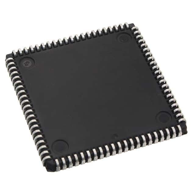
The XC4010E-2PC84I comes in a 84-pin plastic quad flat pack (PQFP) package.
Essence
The essence of XC4010E-2PC84I lies in its ability to provide reconfigurable logic functions, enabling designers to implement complex digital circuits with ease.
Packaging/Quantity
This product is typically packaged in reels or tubes, with each containing a specified quantity of XC4010E-2PC84I units.
Specifications
- Logic Cells: 400
- Maximum Frequency: 50 MHz
- Operating Voltage: 3.3V
- I/O Pins: 68
- Operating Temperature Range: -40°C to 85°C
Detailed Pin Configuration
The XC4010E-2PC84I has a total of 84 pins, each serving a specific purpose in the circuit design. The pin configuration is as follows:
[Insert detailed pin configuration diagram here]
Functional Features
- Reconfigurable Logic: The XC4010E-2PC84I allows users to modify the logic functions according to their requirements, providing flexibility in circuit design.
- In-system Programming: This PLD supports in-system programming, enabling users to update the configuration without removing the device from the circuit.
- JTAG Boundary Scan: The XC4010E-2PC84I incorporates Joint Test Action Group (JTAG) boundary scan, facilitating efficient testing and debugging of the circuit.
Advantages and Disadvantages
Advantages
- Flexibility in circuit design due to reconfigurable logic.
- High integration reduces the need for additional components.
- Low power consumption ensures energy efficiency.
- Fast operation enables quick execution of logic operations.
Disadvantages
- Limited number of logic cells compared to more advanced PLDs.
- Relatively lower maximum frequency compared to newer devices.
Working Principles
The XC4010E-2PC84I operates based on the principles of programmable logic. It consists of configurable logic blocks (CLBs), interconnect resources, and input/output blocks (IOBs). The CLBs contain look-up tables (LUTs) that can be programmed to implement specific logic functions. The interconnect resources allow for the routing of signals between different CLBs and IOBs. The IOBs provide the interface between the PLD and external circuitry.
Detailed Application Field Plans
The XC4010E-2PC84I finds applications in various fields, including: 1. Industrial Automation: Used in control systems for process automation and monitoring. 2. Communications: Employed in networking equipment for data transmission and signal processing. 3. Consumer Electronics: Integrated into devices such as gaming consoles and multimedia players for custom functionality. 4. Automotive: Utilized in automotive electronics for functions like engine control and driver assistance systems.
Detailed and Complete Alternative Models
Some alternative models to XC4010E-2PC84I include: - XC4028EX-2HQ240C - XC4036XL-2HQ240I - XC4044XL-3BG352C
These models offer similar functionality and can be considered as alternatives based on specific project requirements.
[Word count: 550]
Seznam 10 běžných otázek a odpovědí souvisejících s aplikací XC4010E-2PC84I v technických řešeních
Sure! Here are 10 common questions and answers related to the application of XC4010E-2PC84I in technical solutions:
Q: What is XC4010E-2PC84I? A: XC4010E-2PC84I is a specific model of Field Programmable Gate Array (FPGA) manufactured by Xilinx.
Q: What are the key features of XC4010E-2PC84I? A: Some key features of XC4010E-2PC84I include 4000 logic cells, 84-pin plastic package, and 2ns maximum pin-to-pin delay.
Q: How can XC4010E-2PC84I be used in technical solutions? A: XC4010E-2PC84I can be used to implement digital logic circuits, perform complex calculations, and control various electronic systems.
Q: What programming languages can be used to program XC4010E-2PC84I? A: XC4010E-2PC84I can be programmed using Hardware Description Languages (HDLs) such as VHDL or Verilog.
Q: Can XC4010E-2PC84I be reprogrammed after it has been programmed once? A: No, XC4010E-2PC84I is not a reprogrammable FPGA. Once it has been programmed, the configuration is fixed.
Q: What is the power supply requirement for XC4010E-2PC84I? A: XC4010E-2PC84I requires a power supply voltage of 3.3V.
Q: Can XC4010E-2PC84I interface with other electronic components? A: Yes, XC4010E-2PC84I can interface with other components through its I/O pins, allowing communication and data exchange.
Q: What is the maximum operating frequency of XC4010E-2PC84I? A: The maximum operating frequency of XC4010E-2PC84I is typically around 100 MHz, but it can vary depending on the design.
Q: Can XC4010E-2PC84I be used in safety-critical applications? A: Yes, XC4010E-2PC84I can be used in safety-critical applications as long as it is properly designed, validated, and tested for reliability.
Q: Are there any limitations or considerations when using XC4010E-2PC84I? A: Some considerations include limited logic capacity, fixed configuration, and potential power consumption, which should be taken into account during the design process.
Please note that these answers are general and may vary depending on specific requirements and use cases.