

Viz Specifikace pro podrobnosti o produktu.
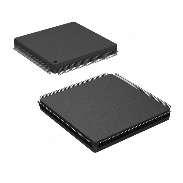
XC4013XL-3PQ208C
Product Overview
Category
XC4013XL-3PQ208C belongs to the category of Field Programmable Gate Arrays (FPGAs).
Use
This product is primarily used in digital circuit design and implementation. FPGAs provide a flexible and customizable solution for various applications, including telecommunications, automotive, aerospace, and consumer electronics.
Characteristics
- High integration: XC4013XL-3PQ208C offers a large number of logic elements, allowing complex designs to be implemented on a single chip.
- Reconfigurability: FPGAs can be reprogrammed multiple times, enabling rapid prototyping and design iterations.
- Parallel processing: The parallel architecture of FPGAs allows for efficient execution of multiple tasks simultaneously.
- Low power consumption: XC4013XL-3PQ208C is designed to minimize power consumption while maintaining high performance.
Package and Quantity
XC4013XL-3PQ208C is packaged in a PQ208C package, which refers to a plastic quad flat pack with 208 pins. The quantity per package depends on the manufacturer's specifications.
Specifications
- Logic Elements: XC4013XL-3PQ208C offers 4000 logic cells.
- Flip-Flops: It provides 1920 flip-flops for storing data.
- Block RAM: This FPGA includes 36 kilobits of block RAM for data storage.
- I/O Pins: XC4013XL-3PQ208C has 104 input/output pins for interfacing with external devices.
- Clock Management: It features built-in clock management resources for precise timing control.
Pin Configuration
The detailed pin configuration of XC4013XL-3PQ208C can be found in the manufacturer's datasheet or reference manual.
Functional Features
XC4013XL-3PQ208C offers the following functional features: - Programmable logic cells for implementing custom digital circuits. - Dedicated arithmetic and logical units for efficient mathematical operations. - Built-in memory blocks for data storage and retrieval. - Flexible I/O pins for interfacing with external devices. - Clock management resources for precise timing control.
Advantages and Disadvantages
Advantages
- Flexibility: FPGAs allow for rapid prototyping and design iterations, making them suitable for dynamic applications.
- High integration: XC4013XL-3PQ208C provides a large number of logic elements on a single chip, enabling complex designs.
- Parallel processing: The parallel architecture of FPGAs allows for efficient execution of multiple tasks simultaneously.
Disadvantages
- Complexity: Designing and programming FPGAs require specialized knowledge and expertise.
- Cost: FPGAs can be more expensive compared to other programmable logic devices.
- Power consumption: While efforts have been made to reduce power consumption, FPGAs still consume more power compared to dedicated ASICs.
Working Principles
XC4013XL-3PQ208C operates based on the principles of reconfigurable computing. It consists of an array of configurable logic cells interconnected through programmable routing resources. These logic cells can be programmed to implement various digital functions, allowing for the creation of custom circuits. The configuration of the FPGA is stored in internal memory or loaded from an external source.
Detailed Application Field Plans
XC4013XL-3PQ208C finds applications in various fields, including: 1. Telecommunications: Used in base stations, network switches, and routers for signal processing and protocol implementation. 2. Automotive: Employed in automotive electronics for engine control, driver assistance systems, and infotainment systems. 3. Aerospace: Utilized in satellite communication systems, avionics, and navigation equipment. 4. Consumer Electronics: Integrated into high-definition televisions, gaming consoles, and audio/video processing devices.
Detailed Alternative Models
- XC4010XL-3PQ208C: A lower-capacity FPGA from the same family, offering 1000 logic cells.
- XC4028XL-3PQ208C: A higher-capacity FPGA with 8000 logic cells, suitable for more complex designs.
- XC4005XL-3PQ208C: A cost-effective option with 500 logic cells, ideal for smaller-scale applications.
In conclusion, XC4013XL-3PQ208C is a versatile FPGA that offers high integration, reconfigurability, and parallel processing capabilities. It finds applications in various industries and can be used for implementing custom digital circuits. While it requires specialized knowledge and expertise, its flexibility and performance make it a valuable tool in the field of digital circuit design.
Seznam 10 běžných otázek a odpovědí souvisejících s aplikací XC4013XL-3PQ208C v technických řešeních
Sure! Here are 10 common questions and answers related to the application of XC4013XL-3PQ208C in technical solutions:
Question: What is XC4013XL-3PQ208C?
Answer: XC4013XL-3PQ208C is a specific model of Field Programmable Gate Array (FPGA) manufactured by Xilinx.Question: What are the key features of XC4013XL-3PQ208C?
Answer: Some key features of XC4013XL-3PQ208C include 4000 logic cells, 192 I/O pins, 36Kbits of block RAM, and support for various communication protocols.Question: In which technical solutions can XC4013XL-3PQ208C be used?
Answer: XC4013XL-3PQ208C can be used in a wide range of applications such as digital signal processing, embedded systems, robotics, telecommunications, and industrial automation.Question: What programming languages can be used to program XC4013XL-3PQ208C?
Answer: XC4013XL-3PQ208C can be programmed using Hardware Description Languages (HDLs) such as VHDL or Verilog.Question: Can XC4013XL-3PQ208C be reprogrammed after initial configuration?
Answer: Yes, XC4013XL-3PQ208C is a reprogrammable FPGA, allowing for flexibility in design changes and updates.Question: What tools are available for designing with XC4013XL-3PQ208C?
Answer: Xilinx provides software tools like Vivado Design Suite that enable designers to create, simulate, and implement designs for XC4013XL-3PQ208C.Question: What is the power supply requirement for XC4013XL-3PQ208C?
Answer: XC4013XL-3PQ208C typically operates at a voltage range of 1.8V to 3.3V, depending on the specific design requirements.Question: Can XC4013XL-3PQ208C interface with other components or devices?
Answer: Yes, XC4013XL-3PQ208C supports various communication protocols like SPI, I2C, UART, and Ethernet, allowing it to interface with other components or devices.Question: Are there any limitations or constraints when using XC4013XL-3PQ208C?
Answer: XC4013XL-3PQ208C has a limited number of logic cells, I/O pins, and memory resources, so designers need to carefully manage their design to fit within these constraints.Question: Where can I find more information about XC4013XL-3PQ208C and its applications?
Answer: You can refer to Xilinx's official website, technical documentation, application notes, or consult with Xilinx experts for more detailed information about XC4013XL-3PQ208C and its applications.
Please note that the answers provided here are general and may vary based on specific design requirements and application scenarios.