

Viz Specifikace pro podrobnosti o produktu.
XC4VLX40-11FF1148I
Product Overview
Category
The XC4VLX40-11FF1148I belongs to the category of Field Programmable Gate Arrays (FPGAs).
Use
FPGAs are integrated circuits that can be programmed and reprogrammed to perform various digital functions. The XC4VLX40-11FF1148I is specifically designed for high-performance applications that require complex logic functions.
Characteristics
- High-density programmable logic device
- Advanced architecture for efficient performance
- Flexible and customizable design
- Low power consumption
- Fast processing speed
- Wide range of I/O options
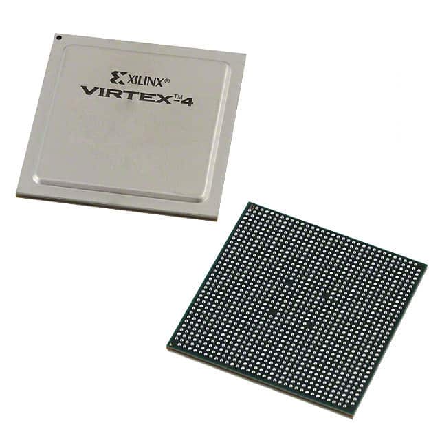
Package
The XC4VLX40-11FF1148I comes in a Flip-Chip FineLine BGA package, which provides excellent thermal performance and reliability.
Essence
The essence of the XC4VLX40-11FF1148I lies in its ability to provide designers with a versatile and powerful platform for implementing complex digital systems.
Packaging/Quantity
The XC4VLX40-11FF1148I is typically packaged individually and is available in various quantities depending on the manufacturer's specifications.
Specifications
- Logic Cells: 40,960
- CLB Flip-Flops: 81,920
- Block RAM: 1,152 Kbits
- DSP Slices: 240
- Maximum Frequency: 550 MHz
- Operating Voltage: 1.2V
- Operating Temperature: -40°C to 100°C
Detailed Pin Configuration
The XC4VLX40-11FF1148I has a complex pin configuration with numerous input/output pins. For detailed information, please refer to the manufacturer's datasheet.
Functional Features
- High-speed data processing
- Configurable logic blocks for flexible design implementation
- Dedicated DSP slices for efficient signal processing
- On-chip memory blocks for data storage
- Built-in clock management resources
- Support for various communication protocols
Advantages and Disadvantages
Advantages
- Versatile and customizable design options
- High-performance capabilities
- Low power consumption
- Fast development time
- Suitable for a wide range of applications
Disadvantages
- Complex programming and configuration process
- Limited availability of alternative models
- Higher cost compared to other programmable logic devices
Working Principles
The XC4VLX40-11FF1148I operates based on the principles of reconfigurable computing. It consists of an array of configurable logic blocks interconnected through programmable routing resources. The device can be programmed using Hardware Description Languages (HDL) such as VHDL or Verilog, allowing designers to define the desired functionality.
Once programmed, the XC4VLX40-11FF1148I executes the specified logic functions by routing signals through the configured interconnections. This enables the device to perform complex digital operations with high speed and efficiency.
Detailed Application Field Plans
The XC4VLX40-11FF1148I finds applications in various fields, including:
- Telecommunications: Used in network routers, switches, and base stations for high-speed data processing and protocol handling.
- Aerospace and Defense: Employed in radar systems, avionics, and military communication equipment for signal processing and control functions.
- Industrial Automation: Utilized in programmable logic controllers (PLCs) and industrial control systems for real-time monitoring and control of manufacturing processes.
- Medical Devices: Integrated into medical imaging systems, patient monitoring devices, and laboratory equipment for data acquisition and processing.
- Automotive: Applied in advanced driver-assistance systems (ADAS), infotainment systems, and engine control units (ECUs) for efficient data processing and control.
Detailed and Complete Alternative Models
While the XC4VLX40-11FF1148I offers a comprehensive set of features, there are alternative models available from other FPGA manufacturers. Some notable alternatives include:
- Altera Cyclone V: Offers similar performance and flexibility with a different architecture.
- Lattice ECP5: Provides low-power options with advanced DSP capabilities.
- Xilinx Spartan-6: Offers a cost-effective solution for less demanding applications.
These alternative models can be considered based on specific project requirements and design constraints.
In conclusion, the XC4VLX40-11FF1148I is a high-performance FPGA that provides designers with a versatile platform for implementing complex digital systems. With its advanced architecture, customizable design options, and wide range of applications, it serves as a powerful tool in various industries.
Seznam 10 běžných otázek a odpovědí souvisejících s aplikací XC4VLX40-11FF1148I v technických řešeních
Sure! Here are 10 common questions and answers related to the application of XC4VLX40-11FF1148I in technical solutions:
Question: What is XC4VLX40-11FF1148I?
- Answer: XC4VLX40-11FF1148I is a field-programmable gate array (FPGA) manufactured by Xilinx. It is part of the Virtex-4 LX family and has 40,000 logic cells.Question: What are the key features of XC4VLX40-11FF1148I?
- Answer: Some key features of XC4VLX40-11FF1148I include high-performance logic fabric, built-in block RAM, DSP slices, and support for various I/O standards.Question: What are the typical applications of XC4VLX40-11FF1148I?
- Answer: XC4VLX40-11FF1148I is commonly used in applications such as telecommunications, networking, industrial automation, video processing, and high-performance computing.Question: How can XC4VLX40-11FF1148I be programmed?
- Answer: XC4VLX40-11FF1148I can be programmed using Xilinx's Vivado or ISE Design Suite software tools. These tools allow users to design and implement their custom logic circuits on the FPGA.Question: What is the maximum clock frequency supported by XC4VLX40-11FF1148I?
- Answer: The maximum clock frequency supported by XC4VLX40-11FF1148I depends on the specific design and implementation. However, it is capable of operating at high speeds, typically in the range of hundreds of megahertz to a few gigahertz.Question: Can XC4VLX40-11FF1148I interface with external devices?
- Answer: Yes, XC4VLX40-11FF1148I supports various I/O standards such as LVCMOS, LVTTL, LVDS, and differential signaling. This allows it to interface with a wide range of external devices and peripherals.Question: Does XC4VLX40-11FF1148I have built-in memory?
- Answer: Yes, XC4VLX40-11FF1148I has built-in block RAM (BRAM) resources that can be used for storing data or implementing memory-intensive functions in the FPGA design.Question: What is the power consumption of XC4VLX40-11FF1148I?
- Answer: The power consumption of XC4VLX40-11FF1148I depends on factors such as the operating frequency, utilization of resources, and specific design implementation. It is recommended to refer to the datasheet for detailed power specifications.Question: Can XC4VLX40-11FF1148I be reprogrammed multiple times?
- Answer: Yes, XC4VLX40-11FF1148I is a reprogrammable FPGA, which means it can be programmed and reprogrammed multiple times to implement different designs or make changes to the existing design.Question: Are there any development boards available for XC4VLX40-11FF1148I?
- Answer: Yes, Xilinx offers development boards like the ML403 and ML410 that are compatible with XC4VLX40-11FF1148I. These boards provide a platform for prototyping and testing designs using the FPGA.
Please note that the answers provided here are general and may vary depending on specific requirements and use cases. It is always recommended to refer to the official documentation and datasheets for accurate and up-to-date information.