

Viz Specifikace pro podrobnosti o produktu.
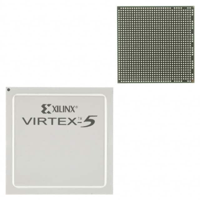
XC5VLX50-1FFG1153CES
Product Overview
Category
XC5VLX50-1FFG1153CES belongs to the category of Field Programmable Gate Arrays (FPGAs).
Use
FPGAs are integrated circuits that can be programmed and reprogrammed to perform various digital functions. They are widely used in industries such as telecommunications, automotive, aerospace, and consumer electronics.
Characteristics
XC5VLX50-1FFG1153CES is a high-performance FPGA with advanced features. It offers a large number of logic cells, high-speed I/O interfaces, and flexible configuration options. This FPGA is designed to handle complex digital designs and provide efficient solutions for demanding applications.
Package
XC5VLX50-1FFG1153CES comes in a compact package that ensures easy integration into electronic systems. The package type is BGA (Ball Grid Array), which provides reliable electrical connections and thermal dissipation.
Essence
The essence of XC5VLX50-1FFG1153CES lies in its ability to provide programmable logic resources that can be customized to meet specific application requirements. It allows designers to implement complex digital circuits without the need for custom-designed ASICs (Application-Specific Integrated Circuits).
Packaging/Quantity
XC5VLX50-1FFG1153CES is typically sold in reels or trays, depending on the manufacturer's packaging standards. The quantity per package may vary, but it is commonly available in quantities suitable for both prototyping and production purposes.
Specifications
- Logic Cells: 48,576
- Block RAM: 2,592 Kbits
- DSP Slices: 240
- Maximum Frequency: 550 MHz
- I/O Pins: 576
- Operating Voltage: 1.2V
- Configuration Memory: 4Mbit PROM
Detailed Pin Configuration
The detailed pin configuration of XC5VLX50-1FFG1153CES can be found in the manufacturer's datasheet. It provides information about the specific functions and connections of each pin, enabling designers to interface the FPGA with other components effectively.
Functional Features
XC5VLX50-1FFG1153CES offers several functional features that make it a versatile choice for various applications:
- High Logic Capacity: With 48,576 logic cells, this FPGA can handle complex digital designs.
- Flexible I/O Interfaces: The 576 I/O pins provide connectivity options for interfacing with external devices.
- High-Speed Serial Transceivers: XC5VLX50-1FFG1153CES supports high-speed serial communication protocols, making it suitable for applications requiring fast data transfer.
- Embedded Memory: The 2,592 Kbits of block RAM allows for efficient storage and retrieval of data within the FPGA.
- DSP Slices: The 240 DSP slices enable efficient implementation of digital signal processing algorithms.
Advantages and Disadvantages
Advantages
- Versatility: XC5VLX50-1FFG1153CES can be programmed to perform a wide range of functions, making it suitable for diverse applications.
- Reconfigurability: FPGAs can be reprogrammed multiple times, allowing for design changes and updates without the need for hardware modifications.
- Time-to-Market: Using an FPGA like XC5VLX50-1FFG1153CES can significantly reduce development time compared to custom ASICs.
Disadvantages
- Power Consumption: FPGAs tend to consume more power compared to dedicated ASICs, which may be a concern in power-sensitive applications.
- Complexity: Designing for FPGAs requires specialized knowledge and tools, making it more challenging than traditional microcontroller-based designs.
Working Principles
XC5VLX50-1FFG1153CES operates based on the principles of reconfigurable logic. The FPGA consists of an array of configurable logic blocks interconnected through programmable routing resources. These logic blocks can be programmed to implement various digital functions, and the interconnections can be configured to establish desired signal paths.
The configuration data is stored in a non-volatile memory (such as a PROM) and loaded into the FPGA during startup. Once configured, the FPGA operates as per the programmed logic, processing input signals and generating output signals based on the defined functionality.
Detailed Application Field Plans
XC5VLX50-1FFG1153CES finds applications in various fields, including:
- Telecommunications: Used in base stations, routers, and network switches for high-speed data processing and protocol handling.
- Automotive: Employed in advanced driver-assistance systems (ADAS), infotainment systems, and engine control units (ECUs) for real-time processing and control.
- Aerospace: Utilized in avionics systems, satellite communication, and radar systems for high-performance signal processing and data handling.
Seznam 10 běžných otázek a odpovědí souvisejících s aplikací XC5VLX50-1FFG1153CES v technických řešeních
Sure! Here are 10 common questions and answers related to the application of XC5VLX50-1FFG1153CES in technical solutions:
Q1: What is XC5VLX50-1FFG1153CES? A1: XC5VLX50-1FFG1153CES is a specific model of Xilinx Virtex-5 FPGA (Field-Programmable Gate Array) that offers advanced programmable logic capabilities for various technical applications.
Q2: What are the key features of XC5VLX50-1FFG1153CES? A2: Some key features of XC5VLX50-1FFG1153CES include 50,000 logic cells, high-speed serial transceivers, embedded PowerPC processors, on-chip memory, and support for various communication protocols.
Q3: What are the typical applications of XC5VLX50-1FFG1153CES? A3: XC5VLX50-1FFG1153CES can be used in a wide range of applications such as telecommunications, aerospace, defense, industrial automation, medical devices, and high-performance computing.
Q4: How can XC5VLX50-1FFG1153CES be programmed? A4: XC5VLX50-1FFG1153CES can be programmed using Xilinx's Vivado Design Suite or ISE Design Suite software tools, which provide a graphical interface for designing and implementing custom logic circuits.
Q5: What is the power consumption of XC5VLX50-1FFG1153CES? A5: The power consumption of XC5VLX50-1FFG1153CES depends on the specific configuration and operating conditions. It is recommended to refer to the datasheet or consult Xilinx's documentation for detailed power consumption information.
Q6: Can XC5VLX50-1FFG1153CES interface with other devices? A6: Yes, XC5VLX50-1FFG1153CES supports various communication protocols such as PCIe, Ethernet, USB, and serial interfaces. It can interface with other devices through these protocols.
Q7: What is the maximum operating frequency of XC5VLX50-1FFG1153CES? A7: The maximum operating frequency of XC5VLX50-1FFG1153CES depends on the specific design and implementation. It is recommended to refer to the datasheet or consult Xilinx's documentation for detailed frequency specifications.
Q8: Can XC5VLX50-1FFG1153CES be used in safety-critical applications? A8: XC5VLX50-1FFG1153CES can be used in safety-critical applications, but additional measures may be required to ensure compliance with relevant safety standards and regulations. It is recommended to consult Xilinx's documentation and seek expert advice for such applications.
Q9: Are there any development boards available for XC5VLX50-1FFG1153CES? A9: Yes, Xilinx offers development boards specifically designed for Virtex-5 FPGAs, including XC5VLX50-1FFG1153CES. These development boards provide a platform for prototyping and testing designs using the FPGA.
Q10: Where can I find technical support for XC5VLX50-1FFG1153CES? A10: Xilinx provides technical support through their website, including documentation, application notes, forums, and direct contact options. It is recommended to visit Xilinx's official website for comprehensive technical support resources.
Please note that the answers provided here are general and it is always advisable to refer to the official documentation and consult with experts for specific technical requirements and applications.