

Viz Specifikace pro podrobnosti o produktu.
XC5VLX50-1FFG1153I
Product Overview
Category
The XC5VLX50-1FFG1153I belongs to the category of Field Programmable Gate Arrays (FPGAs).
Use
FPGAs are integrated circuits that can be programmed and reprogrammed to perform various digital functions. The XC5VLX50-1FFG1153I is specifically designed for high-performance applications.
Characteristics
- High-performance FPGA
- Programmable and reprogrammable
- Versatile and flexible
- Suitable for complex digital designs
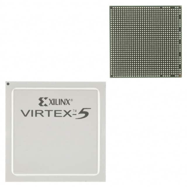
Package
The XC5VLX50-1FFG1153I comes in a specific package known as the Flip Chip FineLine BGA (Ball Grid Array). This package provides excellent thermal performance and allows for easy integration onto circuit boards.
Essence
The essence of the XC5VLX50-1FFG1153I lies in its ability to provide a customizable and high-performance solution for digital design applications.
Packaging/Quantity
The XC5VLX50-1FFG1153I is typically packaged individually and is available in various quantities depending on the requirements of the user or project.
Specifications
- FPGA Family: Virtex-5
- Logic Cells: 48,576
- Slices: 7,680
- Block RAM: 1,728 Kb
- DSP48A1 Slices: 96
- Maximum I/O Pins: 400
- Operating Voltage: 1.2V
- Speed Grade: -1
- Package Type: Flip Chip FineLine BGA
- Package Pins: 1153
Detailed Pin Configuration
The XC5VLX50-1FFG1153I has a total of 1153 pins, each serving a specific purpose in the overall functionality of the FPGA. A detailed pin configuration diagram can be found in the product datasheet.
Functional Features
- High-performance processing capabilities
- Configurable logic cells for custom digital designs
- Integrated memory blocks for efficient data storage
- Dedicated DSP slices for complex mathematical operations
- Flexible I/O pins for interfacing with external devices
Advantages and Disadvantages
Advantages
- Versatile and flexible design options
- High-performance processing capabilities
- Reconfigurable for future updates or changes
- Suitable for complex digital designs
Disadvantages
- Higher cost compared to other programmable logic devices
- Steeper learning curve for programming and utilization
- Limited availability of alternative models with similar specifications
Working Principles
The XC5VLX50-1FFG1153I operates based on the principles of reconfigurable computing. It consists of a matrix of configurable logic cells that can be programmed to perform specific functions. These logic cells are interconnected through a network of programmable interconnects, allowing for the creation of complex digital circuits.
Detailed Application Field Plans
The XC5VLX50-1FFG1153I finds applications in various fields, including:
- Telecommunications: Used in high-speed data transmission systems and network infrastructure.
- Aerospace and Defense: Employed in radar systems, avionics, and military communication equipment.
- Industrial Automation: Utilized in control systems, robotics, and process automation.
- Medical Devices: Integrated into medical imaging systems and diagnostic equipment.
- Research and Development: Used in prototyping and testing of digital designs.
Detailed and Complete Alternative Models
While the XC5VLX50-1FFG1153I offers unique features and specifications, there are alternative models available from the same FPGA family, Virtex-5, that cater to different requirements. Some notable alternatives include:
- XC5VLX30-1FFG665C
- XC5VLX85-1FFG676C
- XC5VLX110-1FFG1153C
These alternative models provide varying logic cell counts, I/O pin configurations, and package options to suit different application needs.
In conclusion, the XC5VLX50-1FFG1153I is a high-performance FPGA belonging to the Virtex-5 family. It offers versatility, flexibility, and customizable features for complex digital designs. While it has advantages such as reconfigurability and high performance, it also has disadvantages like higher cost and limited availability of alternative models with similar specifications. Its applications span across various fields, and there are alternative models available within the same FPGA family to cater to different requirements.
Seznam 10 běžných otázek a odpovědí souvisejících s aplikací XC5VLX50-1FFG1153I v technických řešeních
Sure! Here are 10 common questions and answers related to the application of XC5VLX50-1FFG1153I in technical solutions:
Q1: What is XC5VLX50-1FFG1153I? A1: XC5VLX50-1FFG1153I is a field-programmable gate array (FPGA) manufactured by Xilinx. It is part of the Virtex-5 family and has 50,000 logic cells.
Q2: What are some typical applications of XC5VLX50-1FFG1153I? A2: XC5VLX50-1FFG1153I can be used in various applications such as high-performance computing, telecommunications, aerospace, industrial automation, and image processing.
Q3: What is the maximum operating frequency of XC5VLX50-1FFG1153I? A3: The maximum operating frequency of XC5VLX50-1FFG1153I depends on the specific design and implementation, but it can typically reach frequencies up to several hundred megahertz.
Q4: How much logic capacity does XC5VLX50-1FFG1153I have? A4: XC5VLX50-1FFG1153I has a logic capacity of 50,000 lookup tables (LUTs) or equivalent logic cells.
Q5: What is the power consumption of XC5VLX50-1FFG1153I? A5: The power consumption of XC5VLX50-1FFG1153I depends on the specific design and utilization, but it typically ranges from a few watts to tens of watts.
Q6: Can XC5VLX50-1FFG1153I support multiple I/O standards? A6: Yes, XC5VLX50-1FFG1153I supports multiple I/O standards such as LVCMOS, LVTTL, LVDS, and differential signaling.
Q7: What is the maximum number of I/O pins in XC5VLX50-1FFG1153I? A7: XC5VLX50-1FFG1153I has a maximum of 576 I/O pins.
Q8: Does XC5VLX50-1FFG1153I have built-in memory blocks? A8: Yes, XC5VLX50-1FFG1153I has built-in block RAM (BRAM) resources that can be used for data storage or FIFO implementations.
Q9: Can XC5VLX50-1FFG1153I be reprogrammed after deployment? A9: Yes, XC5VLX50-1FFG1153I is a field-programmable device, which means it can be reprogrammed even after it has been deployed in a system.
Q10: What development tools are available for programming XC5VLX50-1FFG1153I? A10: Xilinx provides various development tools like Vivado Design Suite and ISE Design Suite that can be used to program and configure XC5VLX50-1FFG1153I.
Please note that the answers provided here are general and may vary depending on specific design requirements and implementation details.