

Viz Specifikace pro podrobnosti o produktu.
XC6SLX9-2CSG225C
Product Overview
Category
XC6SLX9-2CSG225C belongs to the category of Field Programmable Gate Arrays (FPGAs).
Use
This product is commonly used in digital circuit design and implementation. FPGAs provide a flexible and customizable solution for various applications, including telecommunications, automotive, aerospace, and consumer electronics.
Characteristics
- High-performance programmable logic device
- Low power consumption
- Large number of configurable logic blocks
- High-speed serial connectivity
- On-chip memory resources
- Flexible I/O options
Package
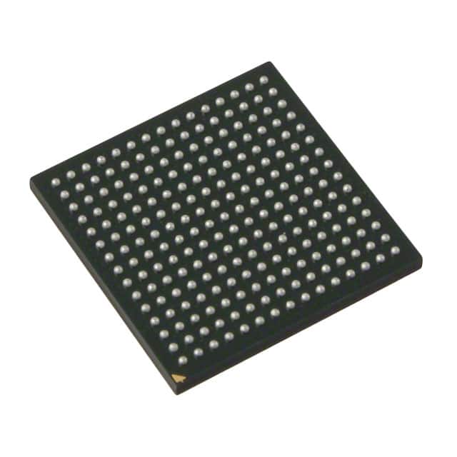
XC6SLX9-2CSG225C is available in a 225-ball chip-scale grid array (CSGA) package.
Essence
The essence of XC6SLX9-2CSG225C lies in its ability to be programmed and reconfigured to perform specific tasks, making it highly versatile and adaptable.
Packaging/Quantity
This product is typically sold individually or in small quantities, depending on the supplier's packaging options.
Specifications
- Logic Cells: 9,152
- Look-Up Tables (LUTs): 5,760
- Flip-Flops: 11,520
- Block RAM: 360 Kb
- DSP Slices: 16
- Maximum Frequency: 400 MHz
- Operating Voltage: 1.2V
- I/O Standards: LVCMOS, LVTTL, HSTL, SSTL, LVDS, RSDS, Mini-LVDS, etc.
- Operating Temperature Range: -40°C to 100°C
Detailed Pin Configuration
The XC6SLX9-2CSG225C FPGA has a total of 225 pins, each serving a specific purpose. The pin configuration includes input/output pins, clock pins, power supply pins, and configuration pins. For a detailed pinout diagram and description, please refer to the product datasheet.
Functional Features
- High-speed data processing capabilities
- Configurable logic blocks for implementing complex digital circuits
- On-chip memory resources for efficient data storage and retrieval
- Flexible I/O options for interfacing with external devices
- Built-in DSP slices for performing mathematical operations
- Support for various communication protocols and standards
Advantages and Disadvantages
Advantages
- Flexibility and reconfigurability
- High-performance computing capabilities
- Low power consumption
- Wide range of I/O standards supported
- On-chip memory resources
Disadvantages
- Higher cost compared to fixed-function integrated circuits
- Steeper learning curve for programming and design
Working Principles
XC6SLX9-2CSG225C operates based on the principles of configurable logic and routing. The FPGA's programmable fabric allows users to define the desired functionality by configuring the interconnections between logic elements. This flexibility enables the FPGA to perform a wide range of tasks, making it suitable for diverse applications.
Detailed Application Field Plans
XC6SLX9-2CSG225C finds applications in various fields, including:
- Telecommunications: Used in base stations, network switches, and routers for high-speed data processing and protocol handling.
- Automotive: Employed in advanced driver assistance systems (ADAS), infotainment systems, and engine control units (ECUs) for real-time data processing and control.
- Aerospace: Utilized in satellite communication systems, avionics, and radar systems for signal processing and control functions.
- Consumer Electronics: Integrated into smart TVs, gaming consoles, and wearable devices for multimedia processing and user interface control.
Detailed and Complete Alternative Models
- XC7A35T-1CPG236C: A newer FPGA model with enhanced performance and additional features.
- XC6SLX16-2CSG324C: Offers higher logic capacity and increased I/O options.
- XC7K70T-1FBG484I: Provides higher performance and larger memory resources.
These alternative models offer varying capabilities and can be considered based on specific project requirements.
In conclusion, the XC6SLX9-2CSG225C FPGA is a versatile and powerful programmable logic device suitable for a wide range of applications. Its flexibility, high-performance computing capabilities, and configurable nature make it an ideal choice for digital circuit design and implementation.
Seznam 10 běžných otázek a odpovědí souvisejících s aplikací XC6SLX9-2CSG225C v technických řešeních
Sure! Here are 10 common questions and answers related to the application of XC6SLX9-2CSG225C in technical solutions:
Question: What is XC6SLX9-2CSG225C?
- Answer: XC6SLX9-2CSG225C is a field-programmable gate array (FPGA) from Xilinx, which is commonly used in various technical solutions.Question: What are the key features of XC6SLX9-2CSG225C?
- Answer: Some key features of XC6SLX9-2CSG225C include a logic capacity of 9,152 slices, 576 Kbits of block RAM, 4 digital clock managers (DCMs), and 92 I/O pins.Question: What are the typical applications of XC6SLX9-2CSG225C?
- Answer: XC6SLX9-2CSG225C is often used in applications such as industrial automation, telecommunications, medical devices, aerospace, and defense.Question: Can XC6SLX9-2CSG225C be used for high-speed data processing?
- Answer: Yes, XC6SLX9-2CSG225C supports high-speed data processing with its built-in DCMs and high-performance logic resources.Question: Is XC6SLX9-2CSG225C suitable for low-power applications?
- Answer: Yes, XC6SLX9-2CSG225C offers power-saving features like dynamic power management and advanced clock gating, making it suitable for low-power applications.Question: Can XC6SLX9-2CSG225C be programmed using industry-standard tools?
- Answer: Yes, XC6SLX9-2CSG225C can be programmed using Xilinx's Vivado Design Suite or ISE Design Suite, which are widely used industry-standard tools.Question: What is the maximum operating frequency of XC6SLX9-2CSG225C?
- Answer: The maximum operating frequency of XC6SLX9-2CSG225C depends on the specific design and implementation, but it can typically reach frequencies of several hundred megahertz (MHz) to a few gigahertz (GHz).Question: Can XC6SLX9-2CSG225C interface with other components or devices?
- Answer: Yes, XC6SLX9-2CSG225C supports various interfaces such as SPI, I2C, UART, Ethernet, and PCIe, allowing it to communicate with other components or devices in a system.Question: Is XC6SLX9-2CSG225C suitable for prototyping or development purposes?
- Answer: Yes, XC6SLX9-2CSG225C is often used for prototyping and development due to its flexibility, reprogrammability, and availability of development tools.Question: Where can I find more information about XC6SLX9-2CSG225C and its applications?
- Answer: You can refer to the official documentation and datasheets provided by Xilinx, as well as online forums and communities dedicated to FPGA development for more information about XC6SLX9-2CSG225C and its applications.
Please note that the answers provided here are general and may vary depending on specific requirements and use cases.