

Viz Specifikace pro podrobnosti o produktu.
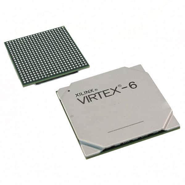
XC6VLX195T-1FFG784C
Product Overview
Category
XC6VLX195T-1FFG784C belongs to the category of Field Programmable Gate Arrays (FPGAs).
Use
FPGAs are integrated circuits that can be programmed and reprogrammed to perform various digital functions. They are widely used in industries such as telecommunications, automotive, aerospace, and consumer electronics.
Characteristics
XC6VLX195T-1FFG784C is a high-performance FPGA with advanced features. It offers a large number of programmable logic cells, high-speed serial transceivers, and embedded memory blocks. These characteristics make it suitable for complex digital designs requiring high processing power and flexibility.
Package
XC6VLX195T-1FFG784C is available in a 784-ball Fine-Pitch Ball Grid Array (FBGA) package. This package provides a compact form factor and excellent thermal performance.
Essence
The essence of XC6VLX195T-1FFG784C lies in its ability to provide a customizable hardware platform for implementing complex digital systems. Its programmability allows designers to create tailored solutions for specific applications.
Packaging/Quantity
XC6VLX195T-1FFG784C is typically sold individually or in reels containing multiple units. The exact quantity depends on the supplier and customer requirements.
Specifications
- Logic Cells: 195,000
- Block RAM: 4,860 Kb
- DSP Slices: 864
- Maximum I/O Pins: 500
- Transceivers: 16
- Operating Voltage: 1.2V
- Operating Temperature Range: -40°C to 100°C
Detailed Pin Configuration
The detailed pin configuration of XC6VLX195T-1FFG784C can be found in the product datasheet provided by the manufacturer. It includes information about power supply pins, I/O pins, configuration pins, and other specialized pins.
Functional Features
XC6VLX195T-1FFG784C offers several functional features that enhance its performance and versatility:
High-Speed Serial Transceivers: The FPGA includes 16 high-speed serial transceivers capable of operating at multi-gigabit rates. These transceivers enable fast data communication between the FPGA and external devices.
Embedded Memory Blocks: The device incorporates a significant amount of embedded memory blocks, allowing for efficient storage and retrieval of data within the FPGA itself. This feature is particularly useful in applications requiring large amounts of on-chip memory.
Flexible I/O Interfaces: XC6VLX195T-1FFG784C supports a wide range of I/O standards, including LVCMOS, LVTTL, LVDS, and differential signaling. This flexibility enables seamless integration with various external devices and interfaces.
Advanced Clock Management: The FPGA includes dedicated clock management resources, such as phase-locked loops (PLLs) and delay-locked loops (DLLs). These resources enable precise control and distribution of clock signals throughout the design.
Advantages and Disadvantages
Advantages
- High processing power and flexibility due to a large number of logic cells.
- Excellent performance in complex digital designs.
- Versatile I/O interfaces for seamless integration with external devices.
- Efficient on-chip memory utilization with embedded memory blocks.
- Advanced clock management capabilities for precise timing control.
Disadvantages
- Relatively high cost compared to other programmable logic devices.
- Steeper learning curve for designers unfamiliar with FPGA programming.
- Higher power consumption compared to simpler digital logic solutions.
Working Principles
XC6VLX195T-1FFG784C operates based on the principles of reconfigurable hardware. The FPGA consists of an array of programmable logic cells interconnected through configurable routing resources. These logic cells can be programmed to implement various digital functions, such as arithmetic operations, data processing, and control logic.
The configuration of the FPGA is stored in non-volatile memory and loaded during startup. Once configured, the FPGA operates autonomously, executing the programmed functionality. The flexibility of FPGAs allows for iterative design changes without requiring physical hardware modifications.
Detailed Application Field Plans
XC6VLX195T-1FFG784C finds applications in various fields, including:
- Telecommunications: Used in high-speed data communication systems, network routers, and switches.
- Automotive: Employed in advanced driver assistance systems (ADAS), infotainment systems, and engine control units (ECUs).
- Aerospace: Utilized in satellite communication systems, avionics, and flight control systems.
- Consumer Electronics: Found in high-definition televisions, gaming consoles, and multimedia devices.
Detailed and Complete Alternative Models
There are several alternative models available in the market that offer similar capabilities to XC6VLX195T-1FFG
Seznam 10 běžných otázek a odpovědí souvisejících s aplikací XC6VLX195T-1FFG784C v technických řešeních
Sure! Here are 10 common questions and answers related to the application of XC6VLX195T-1FFG784C in technical solutions:
1. What is XC6VLX195T-1FFG784C? - XC6VLX195T-1FFG784C is a high-performance field-programmable gate array (FPGA) manufactured by Xilinx. It belongs to the Virtex-6 family and offers advanced features and capabilities.
2. What are the key specifications of XC6VLX195T-1FFG784C? - XC6VLX195T-1FFG784C has 195,000 logic cells, 12.8 Mb of block RAM, 1,920 DSP slices, and a maximum operating frequency of 550 MHz. It also supports various I/O standards and interfaces.
3. What are some typical applications of XC6VLX195T-1FFG784C? - XC6VLX195T-1FFG784C is commonly used in applications such as high-speed data processing, digital signal processing, video and image processing, networking equipment, aerospace and defense systems, and scientific research.
4. How can XC6VLX195T-1FFG784C be programmed? - XC6VLX195T-1FFG784C can be programmed using Xilinx's Vivado Design Suite or ISE Design Suite. These software tools provide a graphical interface and HDL-based design flow for creating and implementing FPGA designs.
5. What are the power requirements for XC6VLX195T-1FFG784C? - XC6VLX195T-1FFG784C requires a core voltage (VCCINT) of 0.95V and an auxiliary voltage (VCCAUX) of 1.8V. The power consumption depends on the design and operating conditions.
6. Can XC6VLX195T-1FFG784C be used in a multi-FPGA system? - Yes, XC6VLX195T-1FFG784C can be used in multi-FPGA systems. It supports various high-speed serial interfaces like PCIe, Ethernet, and Aurora, which enable communication between multiple FPGAs.
7. What are the available I/O standards on XC6VLX195T-1FFG784C? - XC6VLX195T-1FFG784C supports a wide range of I/O standards, including LVCMOS, LVTTL, LVDS, HSTL, SSTL, and differential signaling standards like TMDS and CML.
8. Does XC6VLX195T-1FFG784C have built-in IP cores? - Yes, XC6VLX195T-1FFG784C provides a set of built-in IP cores that can be used to implement common functions like memory controllers, Ethernet MACs, DSP blocks, and more.
9. What is the maximum operating temperature for XC6VLX195T-1FFG784C? - The maximum junction temperature for XC6VLX195T-1FFG784C is 100°C. However, it is recommended to operate the FPGA within a temperature range of 0°C to 85°C for reliable performance.
10. Are there any development boards available for XC6VLX195T-1FFG784C? - Yes, Xilinx offers development boards like the ML605 and VC707 that are compatible with XC6VLX195T-1FFG784C. These boards provide a platform for prototyping and testing FPGA designs.
Please note that the answers provided here are general and may vary depending on specific design requirements and application scenarios.