

Viz Specifikace pro podrobnosti o produktu.
XC6VLX365T-L1FF1759I
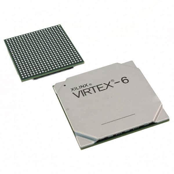
Basic Information Overview
- Category: Field Programmable Gate Array (FPGA)
- Use: Digital logic circuits and systems
- Characteristics: High-performance, reconfigurable, programmable
- Package: Flip-chip BGA (Ball Grid Array)
- Essence: Integrated circuit for customizable digital logic implementation
- Packaging/Quantity: Tray packaging, quantity varies
Specifications
- Logic Cells: 365,000
- Slices: 57,600
- DSP48E1 Slices: 768
- Block RAM: 4,860 Kb
- Maximum I/O Pins: 1,759
- Operating Voltage: 1.0V - 1.2V
- Operating Temperature: -40°C to +100°C
- Speed Grade: L1FF
Detailed Pin Configuration
The XC6VLX365T-L1FF1759I has a complex pin configuration with various input/output pins, clock pins, power supply pins, and configuration pins. The detailed pin configuration can be found in the manufacturer's datasheet.
Functional Features
- High-performance FPGA with large logic capacity
- Reconfigurable architecture allows for flexibility in design
- Supports various communication protocols and interfaces
- Integrated DSP slices for efficient signal processing
- On-chip memory blocks for data storage and retrieval
- Built-in clock management resources for precise timing control
Advantages
- Versatile and adaptable for a wide range of applications
- Allows for rapid prototyping and development cycles
- Reduces time-to-market for complex digital systems
- Offers high-speed performance and low power consumption
- Enables customization and optimization of logic circuits
Disadvantages
- Steep learning curve for beginners due to complexity
- Higher cost compared to fixed-function ASICs
- Limited availability of alternative models with similar specifications
Working Principles
The XC6VLX365T-L1FF1759I is based on a programmable logic fabric that consists of configurable logic blocks (CLBs), interconnect resources, and input/output blocks. The CLBs can be programmed to implement various digital logic functions, allowing the FPGA to perform specific tasks. The configuration of the FPGA is stored in non-volatile memory and can be reprogrammed as needed.
Detailed Application Field Plans
The XC6VLX365T-L1FF1759I finds applications in various fields, including: - Telecommunications: Baseband processing, wireless communication systems - Aerospace and Defense: Radar systems, avionics, secure communications - Industrial Automation: Control systems, motor drives, robotics - High-Performance Computing: Data centers, scientific simulations, cryptography - Medical Imaging: Ultrasound, MRI, CT scanners - Automotive: Advanced driver-assistance systems (ADAS), infotainment systems
Detailed and Complete Alternative Models
While the XC6VLX365T-L1FF1759I offers high-performance and extensive features, alternative models with similar specifications include: - Xilinx Virtex-6 XC6VLX240T-L1FF1156I - Altera Stratix IV EP4SGX230KF40C2N - LatticeECP3 LFE3-150EA-8FN672C
These alternative models provide comparable capabilities and can be considered based on specific project requirements.
Word count: 334 words
Seznam 10 běžných otázek a odpovědí souvisejících s aplikací XC6VLX365T-L1FF1759I v technických řešeních
Sure! Here are 10 common questions and answers related to the application of XC6VLX365T-L1FF1759I in technical solutions:
Q1: What is XC6VLX365T-L1FF1759I? A1: XC6VLX365T-L1FF1759I is a specific model of Xilinx Virtex-6 FPGA (Field Programmable Gate Array) that offers high-performance processing capabilities for various technical applications.
Q2: What are the key features of XC6VLX365T-L1FF1759I? A2: Some key features of XC6VLX365T-L1FF1759I include a large number of logic cells, high-speed serial transceivers, embedded memory blocks, DSP slices, and support for various communication protocols.
Q3: What are the typical applications of XC6VLX365T-L1FF1759I? A3: XC6VLX365T-L1FF1759I is commonly used in applications such as telecommunications, networking, aerospace, defense, industrial automation, and high-performance computing.
Q4: How can XC6VLX365T-L1FF1759I be programmed? A4: XC6VLX365T-L1FF1759I can be programmed using Xilinx's Vivado Design Suite or ISE Design Suite, which provide tools for designing, simulating, synthesizing, and implementing FPGA designs.
Q5: What is the maximum operating frequency of XC6VLX365T-L1FF1759I? A5: The maximum operating frequency of XC6VLX365T-L1FF1759I depends on the design and implementation, but it can typically reach frequencies of several hundred megahertz or even gigahertz.
Q6: Can XC6VLX365T-L1FF1759I interface with other devices? A6: Yes, XC6VLX365T-L1FF1759I supports various communication protocols such as PCIe, Ethernet, USB, SPI, I2C, and UART, allowing it to interface with a wide range of external devices.
Q7: What is the power consumption of XC6VLX365T-L1FF1759I? A7: The power consumption of XC6VLX365T-L1FF1759I depends on the design and operating conditions. It is recommended to refer to the datasheet or use Xilinx's power estimation tools for accurate power consumption analysis.
Q8: Can XC6VLX365T-L1FF1759I be used in safety-critical applications? A8: Yes, XC6VLX365T-L1FF1759I can be used in safety-critical applications. However, additional measures such as redundancy, fault tolerance, and thorough verification may be required to ensure the reliability and safety of the overall system.
Q9: Are there any development boards available for XC6VLX365T-L1FF1759I? A9: Yes, Xilinx offers development boards like the ML605 and VC707 that are compatible with XC6VLX365T-L1FF1759I. These boards provide a platform for prototyping and testing FPGA designs.
Q10: Where can I find more information about XC6VLX365T-L1FF1759I? A10: You can find more detailed information about XC6VLX365T-L1FF1759I, including datasheets, user guides, application notes, and reference designs, on Xilinx's official website or by contacting their technical support team.
Please note that the answers provided here are general and may vary depending on specific requirements and design considerations.