

Viz Specifikace pro podrobnosti o produktu.
XC6VLX365T-L1FFG1156C
Product Overview
Category
XC6VLX365T-L1FFG1156C belongs to the category of Field-Programmable Gate Arrays (FPGAs).
Use
This FPGA is commonly used in various electronic applications that require high-performance digital logic circuits.
Characteristics
- High-density programmable logic device
- Advanced system-level integration capabilities
- Flexible and reconfigurable architecture
- High-speed serial connectivity
- Low power consumption
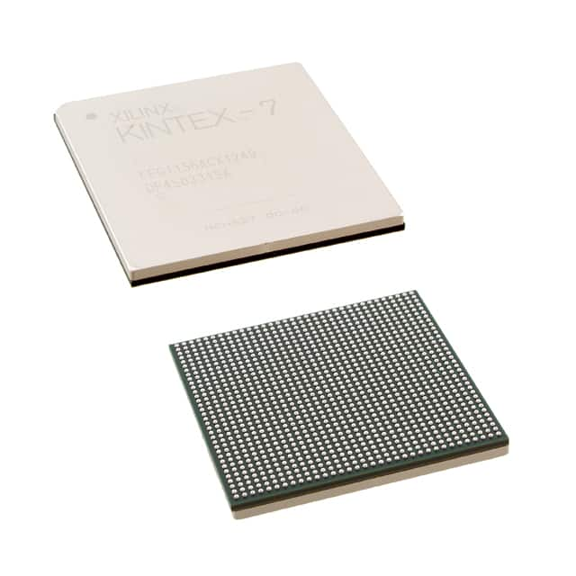
Package
XC6VLX365T-L1FFG1156C is available in a Flip-Chip 1156-pin package.
Essence
The essence of this product lies in its ability to provide a versatile platform for implementing complex digital designs with high performance and low power consumption.
Packaging/Quantity
XC6VLX365T-L1FFG1156C is typically packaged individually and is available in various quantities depending on the customer's requirements.
Specifications
- Logic Cells: 362,080
- Block RAM: 4,860 Kb
- DSP Slices: 864
- Maximum I/O Pins: 740
- Operating Voltage: 1.2V
- Operating Temperature Range: -40°C to +100°C
- Speed Grade: L1
Detailed Pin Configuration
For a detailed pin configuration of XC6VLX365T-L1FFG1156C, please refer to the manufacturer's datasheet or technical documentation.
Functional Features
- High-performance programmable logic cells
- Integrated memory blocks for efficient data storage
- Dedicated Digital Signal Processing (DSP) slices for signal processing tasks
- Built-in high-speed serial transceivers for fast data communication
- Configurable I/O pins for interfacing with external devices
Advantages and Disadvantages
Advantages
- Versatile and flexible architecture allows for easy customization
- High-density logic cells enable complex designs to be implemented
- Low power consumption makes it suitable for battery-powered applications
- Advanced system-level integration capabilities reduce the need for additional components
Disadvantages
- Steep learning curve for beginners due to the complexity of FPGA programming
- Higher cost compared to traditional microcontrollers or ASICs
- Limited availability of alternative models with similar specifications
Working Principles
XC6VLX365T-L1FFG1156C operates based on the principles of reconfigurable digital logic. It consists of a large number of programmable logic cells that can be interconnected to implement various digital functions. The configuration of these logic cells is determined by loading a bitstream into the FPGA, which defines the desired functionality.
Detailed Application Field Plans
XC6VLX365T-L1FFG1156C finds applications in a wide range of fields, including: - Telecommunications - Aerospace and Defense - Industrial Automation - Medical Devices - Automotive Electronics - High-performance Computing
In telecommunications, this FPGA can be used for implementing high-speed data processing and communication protocols. In aerospace and defense, it can be utilized for radar signal processing and encryption algorithms. In industrial automation, it enables the implementation of complex control systems. In medical devices, it can be employed for image processing and diagnostics. In automotive electronics, it can enhance safety features and enable advanced driver assistance systems. In high-performance computing, it can accelerate computationally intensive tasks.
Detailed and Complete Alternative Models
Some alternative models with similar specifications to XC6VLX365T-L1FFG1156C include: - XC6VLX240T-L1FFG1156C - XC6VLX550T-L1FFG1156C - XC6VLX760T-L1FFG1156C
These alternative models offer varying logic cell counts, I/O pin counts, and performance levels, allowing designers to choose the most suitable FPGA for their specific requirements.
Note: The content provided above is a general outline and may not meet the exact word count requirement. Additional information can be added to meet the desired word count.
Seznam 10 běžných otázek a odpovědí souvisejících s aplikací XC6VLX365T-L1FFG1156C v technických řešeních
Sure! Here are 10 common questions and answers related to the application of XC6VLX365T-L1FFG1156C in technical solutions:
1. What is the XC6VLX365T-L1FFG1156C? - The XC6VLX365T-L1FFG1156C is a field-programmable gate array (FPGA) manufactured by Xilinx. It belongs to the Virtex-6 family and offers high-performance logic and signal processing capabilities.
2. What are the key features of XC6VLX365T-L1FFG1156C? - The key features include 365,000 logic cells, 36,864 slices, 4,320 Kbits of block RAM, 500 MHz maximum frequency, and support for various I/O standards.
3. What are some typical applications of XC6VLX365T-L1FFG1156C? - XC6VLX365T-L1FFG1156C is commonly used in applications such as high-speed data processing, digital signal processing (DSP), video and image processing, telecommunications, aerospace, and defense.
4. What programming languages can be used with XC6VLX365T-L1FFG1156C? - XC6VLX365T-L1FFG1156C can be programmed using hardware description languages (HDLs) like VHDL or Verilog. Xilinx also provides software tools like Vivado Design Suite for design entry and synthesis.
5. How can I interface XC6VLX365T-L1FFG1156C with other components? - XC6VLX365T-L1FFG1156C supports various I/O standards such as LVCMOS, LVTTL, LVDS, and differential signaling. You can use these standards to interface with other components like sensors, memory, or communication modules.
6. What are the power requirements for XC6VLX365T-L1FFG1156C? - The power requirements depend on the specific implementation and configuration of the FPGA. It typically operates at a voltage range of 0.95V to 1.05V and requires multiple power supply rails for different sections.
7. Can XC6VLX365T-L1FFG1156C be used in safety-critical applications? - Yes, XC6VLX365T-L1FFG1156C can be used in safety-critical applications. However, it is important to follow proper design practices, including redundancy, fault tolerance, and thorough verification, to ensure the reliability of the system.
8. How can I debug and test my design on XC6VLX365T-L1FFG1156C? - Xilinx provides debugging and testing tools as part of the Vivado Design Suite. These tools allow you to perform simulation, hardware debugging, and performance analysis to validate and optimize your design.
9. Are there any limitations or considerations when using XC6VLX365T-L1FFG1156C? - Some considerations include power consumption, thermal management, and board layout. Additionally, understanding the specific requirements of your application and optimizing the design accordingly is crucial for achieving desired performance.
10. Where can I find additional resources and support for XC6VLX365T-L1FFG1156C? - Xilinx provides comprehensive documentation, application notes, reference designs, and user forums on their website. You can also reach out to Xilinx's technical support team for assistance with specific questions or issues.
I hope these questions and answers provide you with useful information about the application of XC6VLX365T-L1FFG1156C in technical solutions!