

Viz Specifikace pro podrobnosti o produktu.
XC6VSX475T-2FFG1156C
Product Overview
Category
The XC6VSX475T-2FFG1156C belongs to the category of Field Programmable Gate Arrays (FPGAs).
Use
FPGAs are integrated circuits that can be programmed and reprogrammed to perform various digital functions. The XC6VSX475T-2FFG1156C is specifically designed for high-performance applications.
Characteristics
- High-performance FPGA with advanced features
- Large capacity and high-speed processing capabilities
- Flexible and reconfigurable design
- Suitable for complex digital systems
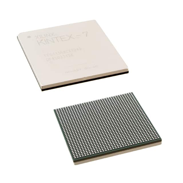
Package
The XC6VSX475T-2FFG1156C comes in a specific package, which ensures its protection during transportation and handling.
Essence
The essence of the XC6VSX475T-2FFG1156C lies in its ability to provide a versatile and powerful platform for implementing complex digital designs.
Packaging/Quantity
The XC6VSX475T-2FFG1156C is typically packaged individually and is available in different quantities depending on the customer's requirements.
Specifications
- FPGA Family: Virtex-6
- Logic Cells: 475,000
- Slices: 29,500
- DSP48A1 Slices: 768
- Block RAM: 4,860 Kb
- Maximum Number of User I/Os: 576
- Operating Voltage: 1.0V
- Operating Temperature Range: -40°C to +100°C
- Package Type: Flip-Chip Fine-Pitch BGA
- Package Pins: 1156
Detailed Pin Configuration
The XC6VSX475T-2FFG1156C has a total of 1156 pins, each serving a specific purpose within the FPGA's architecture. A detailed pin configuration diagram is available in the product's datasheet.
Functional Features
The XC6VSX475T-2FFG1156C offers several functional features that make it suitable for a wide range of applications:
- High-speed serial connectivity
- Advanced memory interfaces
- Flexible clocking options
- Built-in digital signal processing capabilities
- Configurable I/O standards
- On-chip power management
Advantages and Disadvantages
Advantages
- High-performance and large capacity
- Flexibility and reconfigurability
- Support for advanced features and interfaces
- Suitable for complex digital designs
Disadvantages
- Higher cost compared to other FPGA options
- Steeper learning curve for programming and design
Working Principles
The XC6VSX475T-2FFG1156C operates based on the principles of reconfigurable logic. It consists of an array of programmable logic blocks interconnected through configurable routing resources. The user can program the FPGA to implement desired digital functions by configuring the interconnections and functionality of these logic blocks.
Detailed Application Field Plans
The XC6VSX475T-2FFG1156C finds applications in various fields, including:
- Telecommunications: Used in high-speed data transmission systems and network infrastructure.
- Aerospace and Defense: Employed in radar systems, avionics, and secure communication equipment.
- Industrial Automation: Utilized in control systems, robotics, and machine vision applications.
- Medical Devices: Integrated into medical imaging systems and diagnostic equipment.
- Research and Development: Used in prototyping and development of custom digital systems.
Detailed and Complete Alternative Models
- XC7A200T-2FBG484I: Another high-performance FPGA from Xilinx with similar characteristics but a different package and pin configuration.
- Altera Cyclone V GX: A comparable FPGA from Altera (now Intel) with similar features and capabilities.
- Lattice ECP5-85: An alternative FPGA option from Lattice Semiconductor, offering a balance between performance and cost.
These alternative models provide options for users with specific requirements or preferences.
Word count: 511 words
Seznam 10 běžných otázek a odpovědí souvisejících s aplikací XC6VSX475T-2FFG1156C v technických řešeních
Sure! Here are 10 common questions and answers related to the application of XC6VSX475T-2FFG1156C in technical solutions:
Question: What is the XC6VSX475T-2FFG1156C?
Answer: The XC6VSX475T-2FFG1156C is a field-programmable gate array (FPGA) manufactured by Xilinx.Question: What are the key features of the XC6VSX475T-2FFG1156C?
Answer: Some key features include a high logic density, advanced DSP capabilities, multiple I/O standards, and low power consumption.Question: In what applications can the XC6VSX475T-2FFG1156C be used?
Answer: It can be used in various applications such as telecommunications, aerospace, defense, industrial automation, and scientific research.Question: What is the maximum number of logic cells available in the XC6VSX475T-2FFG1156C?
Answer: The XC6VSX475T-2FFG1156C has a maximum of 475,000 logic cells.Question: Can the XC6VSX475T-2FFG1156C support high-speed serial communication protocols?
Answer: Yes, it supports various high-speed serial communication protocols like PCIe, SATA, and Ethernet.Question: What is the operating voltage range for the XC6VSX475T-2FFG1156C?
Answer: The operating voltage range is typically between 1.14V and 1.26V.Question: Does the XC6VSX475T-2FFG1156C have built-in memory?
Answer: No, it does not have built-in memory. However, it can interface with external memory devices.Question: Can the XC6VSX475T-2FFG1156C be reprogrammed after deployment?
Answer: Yes, being an FPGA, the XC6VSX475T-2FFG1156C can be reprogrammed multiple times to implement different designs or updates.Question: What development tools are available for programming the XC6VSX475T-2FFG1156C?
Answer: Xilinx provides a suite of development tools like Vivado Design Suite that allows users to program and configure the FPGA.Question: Are there any specific design considerations when using the XC6VSX475T-2FFG1156C?
Answer: Yes, some considerations include power supply requirements, thermal management, I/O voltage compatibility, and timing constraints.
Please note that the answers provided here are general and may vary depending on specific requirements and application scenarios.