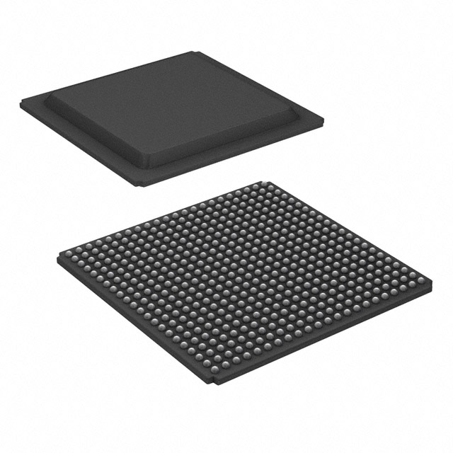
Viz Specifikace pro podrobnosti o produktu.

XC7A100T-1FG484C
Product Overview
Category
XC7A100T-1FG484C belongs to the category of Field Programmable Gate Arrays (FPGAs).
Use
This product is primarily used in digital logic circuits and electronic systems for various applications.
Characteristics
- High-performance FPGA with advanced features
- Flexible and reconfigurable design
- Offers high-speed processing capabilities
- Supports complex algorithms and computations
- Provides efficient power management options
Package
XC7A100T-1FG484C is available in a FG484 package.
Essence
The essence of XC7A100T-1FG484C lies in its ability to provide a customizable hardware platform that can be programmed to perform specific tasks efficiently.
Packaging/Quantity
This product is typically packaged individually and is available in varying quantities depending on the manufacturer's specifications.
Specifications
- FPGA Family: Artix-7
- Logic Cells: 101,440
- CLB Flip-Flops: 63,600
- DSP Slices: 240
- Block RAM: 4,860 Kb
- Maximum I/O Pins: 200
- Operating Voltage: 0.95V - 1.05V
- Operating Temperature: -40°C to +100°C
Detailed Pin Configuration
The detailed pin configuration of XC7A100T-1FG484C can be found in the product datasheet provided by the manufacturer. It includes information about input/output pins, power supply pins, clock pins, and other relevant connections.
Functional Features
- High-speed data processing capabilities
- Configurable logic blocks for custom circuit implementation
- Integrated memory resources for efficient data storage
- Built-in digital signal processing (DSP) slices for complex calculations
- Multiple I/O standards for versatile connectivity options
- On-chip power management features for efficient energy consumption
Advantages and Disadvantages
Advantages
- Flexibility and reconfigurability allow for quick prototyping and design iterations.
- High-performance capabilities enable the implementation of complex algorithms.
- Efficient power management options help optimize energy consumption.
- Availability of a wide range of I/O standards enhances connectivity options.
Disadvantages
- Steep learning curve for beginners due to the complexity of FPGA programming.
- Higher cost compared to other programmable logic devices.
- Limited availability of alternative models with similar specifications.
Working Principles
XC7A100T-1FG484C operates based on the principles of digital logic circuits. It consists of configurable logic blocks (CLBs), interconnect resources, memory elements, and I/O blocks. The CLBs can be programmed to implement custom logic functions, while the interconnect resources facilitate communication between different components. The memory elements store data, and the I/O blocks provide connectivity to external devices. By configuring these elements, the FPGA can perform specific tasks as per the programmed design.
Detailed Application Field Plans
XC7A100T-1FG484C finds applications in various fields, including but not limited to: - Telecommunications - Aerospace and Defense - Industrial Automation - Medical Devices - Automotive Electronics - Data Centers
In telecommunications, this FPGA can be used for signal processing, encryption/decryption, and network protocol implementation. In aerospace and defense, it can be utilized for radar systems, avionics, and secure communications. Industrial automation can benefit from XC7A100T-1FG484C in areas such as control systems, robotics, and machine vision. Medical devices can leverage its capabilities for image processing, patient monitoring, and diagnostics. Automotive electronics can employ this FPGA for advanced driver assistance systems (ADAS) and infotainment. Data centers can utilize it for high-speed data processing, network acceleration, and virtualization.
Detailed and Complete Alternative Models
While XC7A100T-1FG484C is a powerful FPGA, there are alternative models available with similar specifications. Some notable alternatives include: - XC7A100T-2FGG484C - XC7A100T-3CSG324I - XC7A100T-1FTG256C - XC7A100T-1FBG676C
These alternative models offer similar performance and features, but may differ in package type, pin configuration, or other specific characteristics. It is recommended to consult the manufacturer's documentation for detailed information on each alternative model.
Word count: 609 words
Seznam 10 běžných otázek a odpovědí souvisejících s aplikací XC7A100T-1FG484C v technických řešeních
Sure! Here are 10 common questions and answers related to the application of XC7A100T-1FG484C in technical solutions:
Q1: What is XC7A100T-1FG484C? A1: XC7A100T-1FG484C is a field-programmable gate array (FPGA) from Xilinx, which belongs to the Artix-7 family. It has 101,440 logic cells and is housed in a FG484 package.
Q2: What are the key features of XC7A100T-1FG484C? A2: Some key features of XC7A100T-1FG484C include high-performance programmable logic, integrated block RAM, DSP slices, and multiple I/O standards.
Q3: What are the typical applications of XC7A100T-1FG484C? A3: XC7A100T-1FG484C can be used in various applications such as industrial automation, motor control, medical devices, communication systems, and image processing.
Q4: How can XC7A100T-1FG484C be programmed? A4: XC7A100T-1FG484C can be programmed using Xilinx's Vivado Design Suite, which provides a comprehensive development environment for FPGA designs.
Q5: What is the maximum operating frequency of XC7A100T-1FG484C? A5: The maximum operating frequency of XC7A100T-1FG484C depends on the specific design and implementation, but it can typically reach frequencies of several hundred megahertz.
Q6: Can XC7A100T-1FG484C interface with other components or devices? A6: Yes, XC7A100T-1FG484C supports various I/O standards and can interface with other components or devices such as sensors, memory modules, communication interfaces, and display panels.
Q7: Does XC7A100T-1FG484C have built-in memory? A7: Yes, XC7A100T-1FG484C has integrated block RAM (BRAM) resources that can be used for storing data within the FPGA itself.
Q8: Can XC7A100T-1FG484C perform digital signal processing (DSP) tasks? A8: Yes, XC7A100T-1FG484C includes dedicated DSP slices that can be utilized for implementing various DSP algorithms and functions.
Q9: What power supply requirements does XC7A100T-1FG484C have? A9: XC7A100T-1FG484C typically requires a single 1.0V core voltage supply and a separate 3.3V auxiliary voltage supply.
Q10: Are there any development boards available for XC7A100T-1FG484C? A10: Yes, Xilinx offers development boards like the Arty A7-100T, which are specifically designed to support XC7A100T-1FG484C and provide a platform for prototyping and evaluation.
Please note that these answers are general and may vary depending on specific design requirements and implementation details.

