

Viz Specifikace pro podrobnosti o produktu.
XC7K160T-L2FBG484I
Product Overview
Category
XC7K160T-L2FBG484I belongs to the category of Field-Programmable Gate Arrays (FPGAs).
Use
FPGAs are integrated circuits that can be programmed and reprogrammed to perform various digital functions. They are widely used in industries such as telecommunications, automotive, aerospace, and consumer electronics.
Characteristics
XC7K160T-L2FBG484I is known for its high-performance capabilities, flexibility, and scalability. It offers a large number of programmable logic cells, embedded memory blocks, and high-speed I/O interfaces.
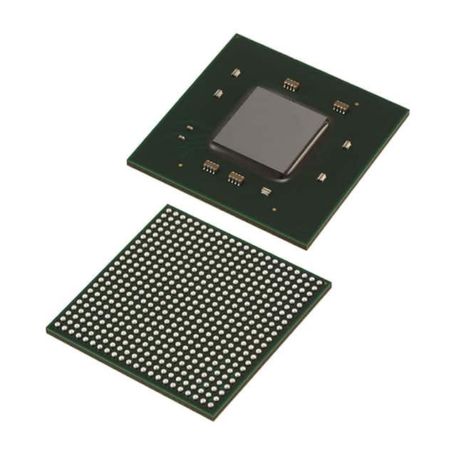
Package
XC7K160T-L2FBG484I comes in a BGA (Ball Grid Array) package, which provides a compact and reliable form factor for mounting on printed circuit boards.
Essence
The essence of XC7K160T-L2FBG484I lies in its ability to provide designers with a versatile platform for implementing complex digital systems. Its programmability allows for rapid prototyping, customization, and adaptability to changing requirements.
Packaging/Quantity
XC7K160T-L2FBG484I is typically sold in trays or reels, with each package containing a specific quantity of devices. The exact packaging and quantity may vary depending on the supplier.
Specifications
- FPGA Family: Kintex-7
- Device Type: XC7K160T
- Logic Cells: 159,200
- Embedded Memory: Up to 36 Mb
- DSP Slices: 720
- Maximum I/O Count: 500
- Operating Voltage: 1.2V
- Operating Temperature Range: -40°C to +100°C
- Package Type: FBG484
- Speed Grade: L2
Detailed Pin Configuration
For a detailed pin configuration of XC7K160T-L2FBG484I, please refer to the manufacturer's datasheet or user guide.
Functional Features
XC7K160T-L2FBG484I offers a range of functional features that make it suitable for various applications:
- High-performance programmable logic cells allow for complex digital circuit implementation.
- Embedded memory blocks provide efficient storage for data processing and buffering.
- High-speed I/O interfaces enable fast communication with external devices.
- DSP slices offer dedicated hardware for performing signal processing tasks.
- Flexible clock management resources support precise timing control.
Advantages and Disadvantages
Advantages
- Versatile and flexible platform for implementing complex digital systems.
- Rapid prototyping and customization capabilities.
- Scalable performance to meet varying application requirements.
- Wide range of available IP cores and development tools.
- Support from a large community of FPGA designers.
Disadvantages
- Steep learning curve for beginners due to the complexity of FPGA programming.
- Higher power consumption compared to other digital integrated circuits.
- Relatively higher cost compared to fixed-function ASICs (Application-Specific Integrated Circuits).
Working Principles
XC7K160T-L2FBG484I operates based on the principles of reconfigurable computing. The FPGA consists of an array of configurable logic blocks interconnected through programmable routing resources. The configuration of these blocks and interconnections is determined by the user's design, which is implemented using a Hardware Description Language (HDL) such as VHDL or Verilog. Upon programming, the FPGA executes the desired digital functions by routing signals through the configured logic blocks.
Detailed Application Field Plans
XC7K160T-L2FBG484I finds applications in various fields, including:
- Telecommunications: Used in base stations, routers, and network switches for high-speed data processing and protocol handling.
- Automotive: Employed in advanced driver-assistance systems (ADAS) for real-time image processing, sensor fusion, and control algorithms.
- Aerospace: Utilized in satellite communication systems, radar signal processing, and flight control systems.
- Consumer Electronics: Integrated into high-definition video processing devices, gaming consoles, and audio equipment for enhanced multimedia experiences.
Detailed and Complete Alternative Models
- XC7K325T-L2FFG900C
- XC7A200T-2FBG484I
- XC6SLX150T-2FGG484C
- XC7Z045-2FFG900I
- XC7VX690T-2FFG1761I
These alternative models offer different combinations of logic capacity, I/O count, and performance characteristics, providing designers with a range of options to suit their specific requirements.
Note: The content provided above is an overview and may not cover all aspects of XC7K160T-L2FBG484I. For detailed technical information, please refer to the manufacturer's documentation.
Seznam 10 běžných otázek a odpovědí souvisejících s aplikací XC7K160T-L2FBG484I v technických řešeních
Sure! Here are 10 common questions and answers related to the application of XC7K160T-L2FBG484I in technical solutions:
Q: What is XC7K160T-L2FBG484I? A: XC7K160T-L2FBG484I is a specific model of Xilinx's Kintex-7 FPGA family, which offers high-performance programmable logic for various applications.
Q: What are the key features of XC7K160T-L2FBG484I? A: Some key features include 160,000 logic cells, high-speed transceivers, embedded memory blocks, DSP slices, and support for various I/O standards.
Q: What are the typical applications of XC7K160T-L2FBG484I? A: XC7K160T-L2FBG484I can be used in a wide range of applications such as wireless communication systems, video processing, industrial control, medical imaging, and aerospace systems.
Q: How can I program XC7K160T-L2FBG484I? A: XC7K160T-L2FBG484I can be programmed using Xilinx's Vivado Design Suite, which provides a comprehensive development environment for FPGA designs.
Q: What are the power requirements for XC7K160T-L2FBG484I? A: The power requirements depend on the specific design and configuration. It is recommended to refer to the datasheet and power estimation tools provided by Xilinx.
Q: Can XC7K160T-L2FBG484I interface with other components or devices? A: Yes, XC7K160T-L2FBG484I supports various interfaces such as PCIe, Ethernet, USB, DDR3 memory, and many more, making it compatible with a wide range of devices.
Q: What is the maximum operating frequency of XC7K160T-L2FBG484I? A: The maximum operating frequency depends on the design and implementation. It is recommended to refer to the datasheet and timing analysis tools provided by Xilinx.
Q: Can XC7K160T-L2FBG484I be used in safety-critical applications? A: Yes, XC7K160T-L2FBG484I can be used in safety-critical applications. However, additional measures such as redundancy and fault-tolerant designs may be required to meet specific safety standards.
Q: Are there any development boards available for XC7K160T-L2FBG484I? A: Yes, Xilinx offers development boards like the Kintex-7 KC705 Evaluation Kit, which provides a platform for prototyping and evaluating designs based on XC7K160T-L2FBG484I.
Q: Where can I find technical documentation and support for XC7K160T-L2FBG484I? A: Xilinx's website provides comprehensive technical documentation, including datasheets, user guides, application notes, and forums where you can seek support from the community or Xilinx experts.
Please note that the answers provided here are general and may vary depending on specific requirements and use cases.