

Viz Specifikace pro podrobnosti o produktu.
XC7K325T-2FF900I
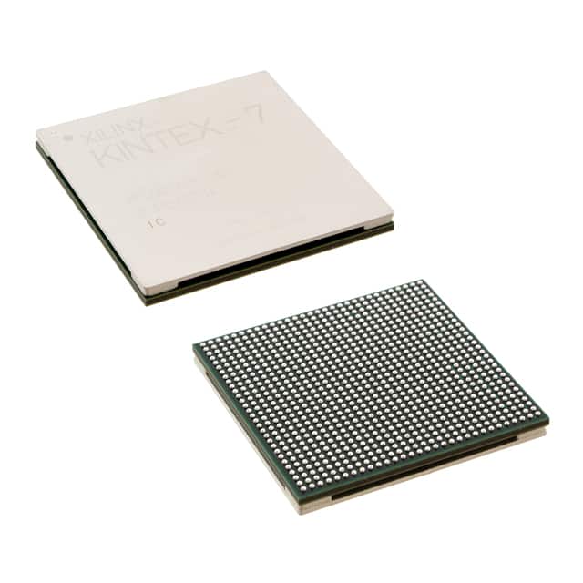
Product Overview
Category
The XC7K325T-2FF900I belongs to the category of Field Programmable Gate Arrays (FPGAs).
Use
FPGAs are integrated circuits that can be programmed and reprogrammed to perform various digital functions. The XC7K325T-2FF900I is specifically designed for high-performance applications that require complex digital processing.
Characteristics
- High-performance FPGA with advanced features
- Large capacity and high-speed processing capabilities
- Flexible and reconfigurable design
- Suitable for a wide range of applications
Package
The XC7K325T-2FF900I comes in a compact package that ensures easy integration into electronic systems. It is designed to be mounted on a printed circuit board (PCB) using surface mount technology (SMT).
Essence
The essence of the XC7K325T-2FF900I lies in its ability to provide a customizable hardware platform for implementing complex digital designs. It offers a high level of performance, flexibility, and reconfigurability.
Packaging/Quantity
The XC7K325T-2FF900I is typically packaged in trays or reels, depending on the manufacturer's specifications. The quantity per package may vary, but it is commonly available in quantities suitable for both prototyping and production purposes.
Specifications
- FPGA Family: Kintex-7
- Device Type: XC7K325T
- Logic Cells: 325,000
- DSP Slices: 1,920
- Block RAM: 36 Mb
- Maximum I/O Pins: 900
- Operating Voltage: 1.0V - 1.2V
- Operating Temperature Range: -40°C to +100°C
Detailed Pin Configuration
The XC7K325T-2FF900I has a comprehensive pin configuration that allows for versatile connectivity. The detailed pinout can be found in the manufacturer's datasheet.
Functional Features
- High-performance processing capabilities
- Configurable logic blocks for implementing complex digital functions
- Dedicated DSP slices for efficient signal processing
- Abundant memory resources for data storage and retrieval
- Flexible I/O interfaces for seamless integration with external devices
- Built-in clock management resources for precise timing control
Advantages and Disadvantages
Advantages
- High processing power and performance
- Flexibility to adapt to changing requirements
- Reconfigurability for iterative design improvements
- Extensive ecosystem support and development tools
- Wide range of available IP cores for accelerated development
Disadvantages
- Higher cost compared to other programmable logic devices
- Steeper learning curve for beginners
- Requires specialized knowledge for optimal utilization
- Limited availability of alternative models with similar specifications
Working Principles
The XC7K325T-2FF900I operates based on the principles of reconfigurable computing. It consists of configurable logic blocks, memory elements, and I/O interfaces interconnected through programmable routing resources. The FPGA can be programmed using hardware description languages (HDLs) such as VHDL or Verilog to define the desired functionality. Upon programming, the FPGA executes the specified digital design by configuring its internal resources accordingly.
Detailed Application Field Plans
The XC7K325T-2FF900I finds applications in various fields that require high-performance digital processing. Some of the key application areas include:
- Communications: Used in wireless base stations, network routers, and communication infrastructure equipment for signal processing and protocol handling.
- Aerospace and Defense: Employed in radar systems, avionics, and military-grade communication systems for real-time data processing and encryption.
- Industrial Automation: Integrated into industrial control systems, robotics, and machine vision applications for high-speed data processing and control.
- Medical Imaging: Utilized in medical imaging devices such as ultrasound machines and MRI scanners for image processing and analysis.
- High-Frequency Trading: Deployed in financial trading systems for low-latency data processing and algorithmic trading strategies.
Detailed and Complete Alternative Models
While the XC7K325T-2FF900I offers a unique combination of features and performance, there are alternative FPGA models available with similar capabilities. Some notable alternatives include:
- Xilinx Virtex-7 series
- Intel (formerly Altera) Stratix V series
- Lattice Semiconductor ECP5 series
- Microsemi SmartFusion2 series
These alternative models provide options for designers to choose based on their specific requirements and preferences.
In conclusion, the XC7K325T-2FF900I is a high-performance FPGA that offers flexibility, reconfigurability, and advanced features. It finds applications in various fields, including communications, aerospace, industrial automation, medical imaging, and high-frequency trading. While it has advantages such as high processing power and ecosystem
Seznam 10 běžných otázek a odpovědí souvisejících s aplikací XC7K325T-2FF900I v technických řešeních
Sure! Here are 10 common questions and answers related to the application of XC7K325T-2FF900I in technical solutions:
Q: What is XC7K325T-2FF900I? A: XC7K325T-2FF900I is a specific model of Xilinx's Kintex-7 FPGA family, which offers high-performance programmable logic for various technical applications.
Q: What are the key features of XC7K325T-2FF900I? A: Some key features include a large number of programmable logic cells, high-speed I/O interfaces, embedded memory blocks, DSP slices, and advanced clocking capabilities.
Q: What are the typical applications of XC7K325T-2FF900I? A: XC7K325T-2FF900I is commonly used in applications such as wireless communication systems, video processing, industrial automation, aerospace, and defense.
Q: How does XC7K325T-2FF900I compare to other FPGA models? A: XC7K325T-2FF900I offers a balance between logic capacity, performance, and power consumption, making it suitable for mid-range to high-end applications compared to other FPGA models.
Q: What development tools are available for programming XC7K325T-2FF900I? A: Xilinx provides Vivado Design Suite, which includes tools for designing, simulating, synthesizing, and programming XC7K325T-2FF900I.
Q: Can XC7K325T-2FF900I be used in safety-critical applications? A: Yes, XC7K325T-2FF900I can be used in safety-critical applications with proper design considerations and adherence to relevant safety standards.
Q: What is the power consumption of XC7K325T-2FF900I? A: The power consumption of XC7K325T-2FF900I depends on the specific design and operating conditions, but it typically ranges from a few watts to tens of watts.
Q: Can XC7K325T-2FF900I interface with other components or devices? A: Yes, XC7K325T-2FF900I supports various high-speed interfaces such as PCIe, Ethernet, USB, DDR3 memory, and can be easily integrated with other components or devices.
Q: Are there any limitations or considerations when using XC7K325T-2FF900I? A: Some considerations include thermal management due to power consumption, proper signal integrity design for high-speed interfaces, and understanding the FPGA's capabilities and limitations.
Q: Where can I find more information about XC7K325T-2FF900I? A: You can refer to Xilinx's official website, product documentation, application notes, and online forums for more detailed information about XC7K325T-2FF900I and its applications.
Please note that the answers provided here are general and may vary depending on specific requirements and design considerations.