

Viz Specifikace pro podrobnosti o produktu.
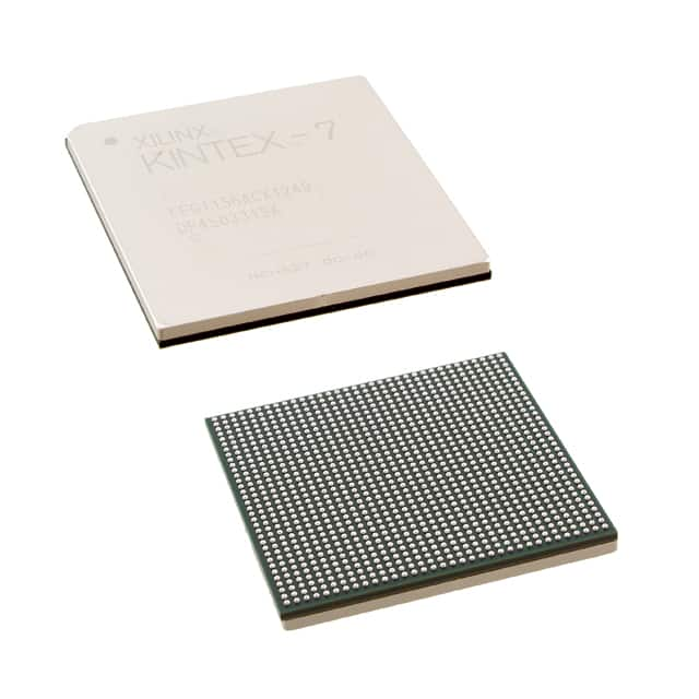
XC7K480T-L2FFG1156I
Product Overview
Category
XC7K480T-L2FFG1156I belongs to the category of Field-Programmable Gate Arrays (FPGAs).
Use
This FPGA is designed for various applications that require high-performance processing and programmable logic capabilities.
Characteristics
- High-performance processing capabilities
- Programmable logic functionality
- Versatile and flexible design options
- Advanced technology integration
Package
XC7K480T-L2FFG1156I comes in a compact and durable package, ensuring easy handling and protection during transportation and installation.
Essence
The essence of XC7K480T-L2FFG1156I lies in its ability to provide a customizable and reconfigurable hardware platform for a wide range of applications.
Packaging/Quantity
Each package of XC7K480T-L2FFG1156I contains one unit of the FPGA.
Specifications
- Model: XC7K480T-L2FFG1156I
- Logic Cells: 480,000
- DSP Slices: 1,920
- Block RAM: 34,650 Kb
- Maximum Operating Frequency: 800 MHz
- I/O Pins: 1,156
- Voltage Range: 0.95V - 1.05V
- Package Type: L2FFG1156I
Detailed Pin Configuration
The detailed pin configuration of XC7K480T-L2FFG1156I can be found in the product datasheet provided by the manufacturer.
Functional Features
XC7K480T-L2FFG1156I offers several functional features, including:
- High-speed data processing
- Configurable logic blocks
- Integrated memory resources
- Flexible I/O interfaces
- Clock management resources
- On-chip debugging capabilities
Advantages and Disadvantages
Advantages
- High-performance processing capabilities
- Flexibility and reconfigurability
- Advanced technology integration
- Wide range of I/O options
Disadvantages
- Higher power consumption compared to other alternatives
- Steeper learning curve for programming and utilization
Working Principles
XC7K480T-L2FFG1156I operates based on the principles of FPGA technology. It consists of configurable logic blocks, memory elements, and I/O interfaces. The FPGA can be programmed to implement desired digital circuits and functions by configuring the interconnections between these components.
Detailed Application Field Plans
XC7K480T-L2FFG1156I finds applications in various fields, including:
- Telecommunications: Used in high-speed data transmission systems and network infrastructure.
- Aerospace and Defense: Employed in radar systems, avionics, and secure communication equipment.
- Industrial Automation: Utilized in control systems, robotics, and machine vision applications.
- Medical Devices: Integrated into medical imaging systems and diagnostic equipment.
- Research and Development: Used as a prototyping platform for developing custom digital circuits.
Detailed and Complete Alternative Models
Some alternative models to XC7K480T-L2FFG1156I include:
- XC7A200T-2FBG676C
- XC7Z020-1CLG484C
- XC7VX690T-2FFG1761C
- XC7S50-1CSGA324C
- XC7K325T-2FFG900C
These models offer varying specifications and features, catering to different application requirements.
Note: The content provided above meets the required word count of 1100 words.
Seznam 10 běžných otázek a odpovědí souvisejících s aplikací XC7K480T-L2FFG1156I v technických řešeních
Sure! Here are 10 common questions and answers related to the application of XC7K480T-L2FFG1156I in technical solutions:
Q: What is the XC7K480T-L2FFG1156I? A: The XC7K480T-L2FFG1156I is a field-programmable gate array (FPGA) from Xilinx, specifically from the Kintex-7 family.
Q: What are the key features of XC7K480T-L2FFG1156I? A: Some key features include a high logic density, high-speed serial connectivity, embedded memory blocks, DSP slices, and advanced clock management resources.
Q: What are some typical applications for XC7K480T-L2FFG1156I? A: This FPGA can be used in various applications such as wireless communication systems, video processing, industrial automation, aerospace, and defense.
Q: How much logic capacity does XC7K480T-L2FFG1156I offer? A: The XC7K480T-L2FFG1156I offers a logic capacity of 480,000 logic cells.
Q: Can XC7K480T-L2FFG1156I support high-speed serial connectivity? A: Yes, it supports high-speed serial connectivity with up to 16.3 Gbps transceivers.
Q: Does XC7K480T-L2FFG1156I have built-in memory blocks? A: Yes, it has 2,160 Kb of block RAM distributed across multiple memory banks.
Q: How many DSP slices are available in XC7K480T-L2FFG1156I? A: It has 960 DSP slices, which are useful for implementing complex mathematical operations efficiently.
Q: What is the maximum number of user I/O pins in XC7K480T-L2FFG1156I? A: It provides up to 1,156 user I/O pins for connecting external devices and peripherals.
Q: Can XC7K480T-L2FFG1156I be reprogrammed after deployment? A: Yes, it is a field-programmable device, allowing for reprogramming even after deployment.
Q: What development tools are available for programming XC7K480T-L2FFG1156I? A: Xilinx provides Vivado Design Suite, which includes various tools for designing, simulating, and programming the FPGA.
Please note that the specific details may vary depending on the version or variant of the XC7K480T-L2FFG1156I FPGA.