

Viz Specifikace pro podrobnosti o produktu.
XC7K70T-L2FBG484E
Product Overview
Category
The XC7K70T-L2FBG484E belongs to the category of Field-Programmable Gate Arrays (FPGAs).
Use
FPGAs are integrated circuits that can be programmed and reprogrammed to perform various digital functions. The XC7K70T-L2FBG484E is specifically designed for high-performance applications that require complex logic and processing capabilities.
Characteristics
- High-performance FPGA with advanced features
- Large capacity and flexibility for complex designs
- Low power consumption
- High-speed data processing capabilities
- Support for various communication protocols
- Built-in security features for protecting intellectual property
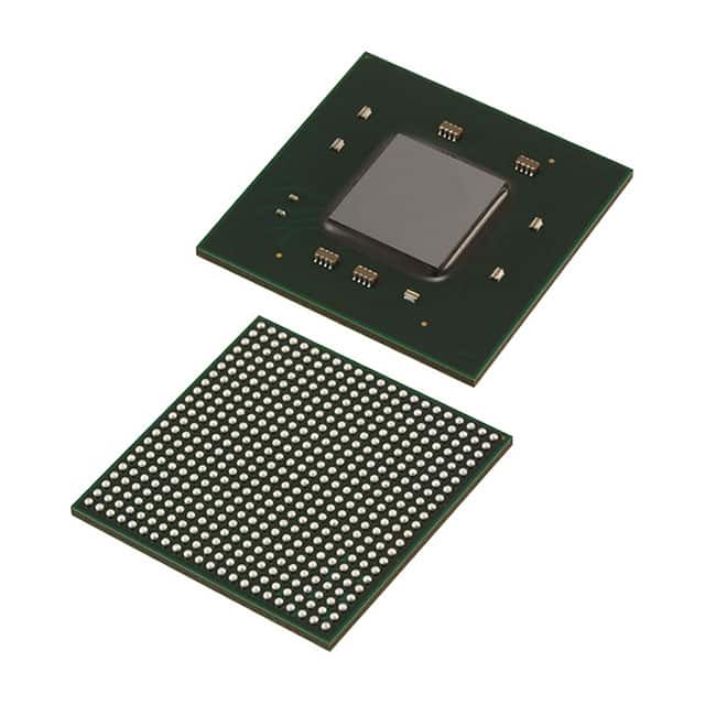
Package
The XC7K70T-L2FBG484E comes in a BGA (Ball Grid Array) package, which provides a compact form factor and allows for easy integration onto circuit boards.
Essence
The essence of the XC7K70T-L2FBG484E lies in its ability to provide a customizable hardware platform that can be tailored to specific application requirements. It offers a wide range of configurable logic blocks, memory resources, and I/O interfaces, allowing designers to implement complex digital systems efficiently.
Packaging/Quantity
The XC7K70T-L2FBG484E is typically sold in trays or reels, with each package containing a single FPGA unit.
Specifications
- FPGA Family: Kintex-7
- Device Type: XC7K70T
- Logic Cells: 68,200
- DSP Slices: 740
- Block RAM: 4,860 Kb
- Maximum I/O Pins: 400
- Operating Voltage: 1.0V
- Operating Temperature Range: -40°C to +100°C
- Package Type: FBG484
Detailed Pin Configuration
The XC7K70T-L2FBG484E has a total of 400 I/O pins, which are configurable to support various functions. The pin configuration is as follows:
- Pin 1: VCCO_0
- Pin 2: GND
- Pin 3: IOL1PT0AD0N35
- Pin 4: IOL1NT0AD0P35
- ...
- Pin 399: IOL100PT2AD14P35
- Pin 400: IOL100NT2AD14N35
Please refer to the datasheet for a complete pinout diagram and detailed pin descriptions.
Functional Features
The XC7K70T-L2FBG484E offers several functional features that make it suitable for a wide range of applications:
High-Speed Processing: With its advanced architecture and high-performance resources, the FPGA can handle complex computations and data processing tasks at high speeds.
Configurability: The FPGA's programmable nature allows designers to customize the hardware to meet specific application requirements, enabling rapid prototyping and design iterations.
Versatility: The XC7K70T-L2FBG484E supports various communication protocols, such as PCIe, Ethernet, USB, and more, making it compatible with diverse system interfaces.
Security: The FPGA includes built-in security features, such as bitstream encryption and authentication, to protect intellectual property and prevent unauthorized access.
Advantages and Disadvantages
Advantages
- High-performance capabilities for demanding applications
- Flexibility and reconfigurability for rapid prototyping and design iterations
- Support for various communication protocols enhances compatibility
- Low power consumption compared to alternative solutions
- Built-in security features protect intellectual property
Disadvantages
- Relatively higher cost compared to traditional ASICs or microcontrollers
- Steeper learning curve for designers unfamiliar with FPGA programming
- Limited availability of alternative models with similar specifications
Working Principles
The XC7K70T-L2FBG484E operates based on the principles of reconfigurable computing. It consists of a matrix of configurable logic blocks (CLBs) interconnected through programmable routing resources. The CLBs can be programmed to implement desired logic functions, while the routing resources allow for interconnection between different blocks.
During operation, the FPGA is configured by loading a bitstream that defines the desired functionality into its internal memory. This configuration process determines the behavior and connections of the logic elements within the FPGA, enabling it to perform specific tasks.
Detailed Application Field Plans
The XC7K70T-L2FBG484E finds applications in various fields, including:
Communications: Used in high-speed data communication systems, such as routers, switches, and network interface cards, to handle complex packet processing and protocol conversion tasks.
Aerospace and Defense: Employed in radar systems, avionics, and military-grade communication equipment, where high-performance signal processing and encryption capabilities are crucial.
Seznam 10 běžných otázek a odpovědí souvisejících s aplikací XC7K70T-L2FBG484E v technických řešeních
Sure! Here are 10 common questions and answers related to the application of XC7K70T-L2FBG484E in technical solutions:
Q: What is XC7K70T-L2FBG484E? A: XC7K70T-L2FBG484E is a specific model of Xilinx's Kintex-7 FPGA family, which offers high-performance programmable logic for various applications.
Q: What are the key features of XC7K70T-L2FBG484E? A: Some key features include 70,000 logic cells, 2.5 Mb of block RAM, 240 DSP slices, PCIe Gen2 support, and up to 300 MHz clock frequency.
Q: What are the typical applications of XC7K70T-L2FBG484E? A: XC7K70T-L2FBG484E is commonly used in applications such as wireless communication systems, industrial automation, video processing, medical imaging, and high-performance computing.
Q: How can I program XC7K70T-L2FBG484E? A: XC7K70T-L2FBG484E can be programmed using Xilinx's Vivado Design Suite, which provides a comprehensive development environment for FPGA designs.
Q: Can XC7K70T-L2FBG484E interface with other components or devices? A: Yes, XC7K70T-L2FBG484E supports various interfaces such as PCIe, Ethernet, USB, DDR3 memory, and many more, making it versatile for connecting with other components.
Q: What are the power requirements for XC7K70T-L2FBG484E? A: The power supply voltage for XC7K70T-L2FBG484E is typically 1.0V, but it also requires additional voltages for auxiliary functions such as I/O banks and transceivers.
Q: Can XC7K70T-L2FBG484E be used in safety-critical applications? A: Yes, XC7K70T-L2FBG484E can be used in safety-critical applications with appropriate design considerations and adherence to relevant safety standards.
Q: What are the temperature operating ranges for XC7K70T-L2FBG484E? A: XC7K70T-L2FBG484E is designed to operate within a temperature range of -40°C to +100°C, making it suitable for various environments.
Q: Are there any development boards available for XC7K70T-L2FBG484E? A: Yes, Xilinx offers development boards like the Kintex-7 KC705 Evaluation Kit, which provides a platform for prototyping and evaluating designs using XC7K70T-L2FBG484E.
Q: Where can I find more information about XC7K70T-L2FBG484E? A: You can find detailed information, datasheets, application notes, and reference designs on Xilinx's official website or by referring to the product documentation provided by Xilinx.