

Viz Specifikace pro podrobnosti o produktu.
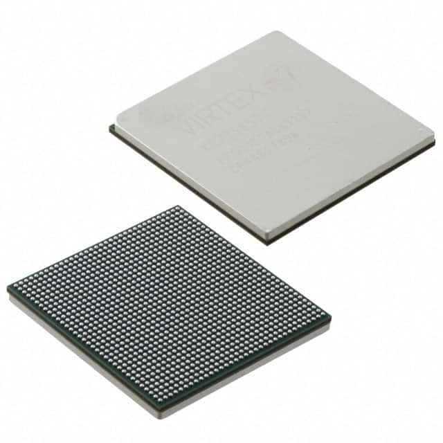
XC7V585T-2FFG1157C
Product Overview
Category
The XC7V585T-2FFG1157C belongs to the category of Field Programmable Gate Arrays (FPGAs).
Use
FPGAs are integrated circuits that can be programmed and reprogrammed to perform various digital functions. The XC7V585T-2FFG1157C is specifically designed for high-performance applications that require complex logic and processing capabilities.
Characteristics
- High-performance FPGA with advanced features
- Large capacity and high-speed processing capabilities
- Flexible and reconfigurable design
- Suitable for demanding applications in industries such as telecommunications, aerospace, and defense
Package
The XC7V585T-2FFG1157C comes in a specific package that ensures proper protection and ease of integration into electronic systems. The package type for this FPGA is FF1157.
Essence
The essence of the XC7V585T-2FFG1157C lies in its ability to provide a highly customizable and powerful solution for digital circuit design and implementation.
Packaging/Quantity
The XC7V585T-2FFG1157C is typically packaged individually and is available in varying quantities depending on the requirements of the customer or project.
Specifications
- FPGA Family: Virtex-7
- Logic Cells: 585,000
- DSP Slices: 1,920
- Block RAM: 36 Mb
- Maximum I/O Pins: 1,157
- Operating Voltage: 1.0V
- Operating Temperature Range: -40°C to +100°C
- Package Type: FF1157
Detailed Pin Configuration
The XC7V585T-2FFG1157C has a comprehensive pin configuration that allows for connectivity with external devices and components. The detailed pin configuration can be found in the product datasheet provided by the manufacturer.
Functional Features
The XC7V585T-2FFG1157C offers several functional features that make it a versatile FPGA for various applications:
- High-speed processing capabilities
- Configurable logic blocks for custom circuit implementation
- Integrated DSP slices for efficient signal processing
- Abundant memory resources for data storage and retrieval
- Flexible I/O interfaces for seamless integration with external devices
- Advanced clock management features for precise timing control
Advantages and Disadvantages
Advantages
- High-performance and large capacity for complex designs
- Reconfigurable nature allows for flexibility in design iterations
- Wide range of integrated features reduces the need for additional components
- Suitable for demanding applications in various industries
Disadvantages
- Higher cost compared to other programmable logic devices
- Steeper learning curve for beginners due to complexity
- Power consumption can be relatively high, requiring proper thermal management
Working Principles
The XC7V585T-2FFG1157C operates based on the principles of digital logic design. It consists of configurable logic blocks (CLBs), interconnect resources, memory elements, and I/O interfaces. The CLBs can be programmed to implement desired logic functions, while the interconnect resources facilitate communication between different parts of the FPGA. Memory elements provide storage capabilities, and the I/O interfaces enable communication with external devices.
Detailed Application Field Plans
The XC7V585T-2FFG1157C finds applications in various fields, including:
- Telecommunications: Used in high-speed data transmission systems, network routers, and switches.
- Aerospace: Employed in satellite communication systems, radar processing, and avionics.
- Defense: Utilized in military-grade communication systems, secure data encryption, and surveillance equipment.
- Industrial Automation: Applied in control systems, robotics, and machine vision applications.
- Medical Devices: Used in medical imaging systems, patient monitoring devices, and diagnostic equipment.
Detailed and Complete Alternative Models
- XC7V2000T-2FFG1156C
- XC7V1000T-2FFG1156C
- XC7V585T-2FFG1761C
- XC7VX690T-2FFG1761C
- XC7VX980T-2FFG1761C
These alternative models offer varying capacities, features, and package options to cater to different project requirements.
Note: The content provided above is a sample structure for an encyclopedia entry and may not reflect the actual specifications or details of the XC7V585T-2FFG1157C FPGA.
Seznam 10 běžných otázek a odpovědí souvisejících s aplikací XC7V585T-2FFG1157C v technických řešeních
Sure! Here are 10 common questions and answers related to the application of XC7V585T-2FFG1157C in technical solutions:
Q: What is XC7V585T-2FFG1157C? A: XC7V585T-2FFG1157C is a specific model of Xilinx Virtex-7 FPGA (Field-Programmable Gate Array) that offers high-performance processing capabilities.
Q: What are the key features of XC7V585T-2FFG1157C? A: Some key features of XC7V585T-2FFG1157C include a large number of programmable logic cells, high-speed serial transceivers, integrated memory blocks, and advanced DSP (Digital Signal Processing) capabilities.
Q: In what applications can XC7V585T-2FFG1157C be used? A: XC7V585T-2FFG1157C can be used in various applications such as aerospace and defense systems, telecommunications infrastructure, high-performance computing, and industrial automation.
Q: How can XC7V585T-2FFG1157C enhance system performance? A: XC7V585T-2FFG1157C can enhance system performance by accelerating complex algorithms, enabling parallel processing, and providing high-speed data transfer capabilities.
Q: Can XC7V585T-2FFG1157C be reprogrammed after deployment? A: Yes, XC7V585T-2FFG1157C is a field-programmable device, which means it can be reprogrammed even after it has been deployed in a system.
Q: What development tools are available for programming XC7V585T-2FFG1157C? A: Xilinx provides Vivado Design Suite, which is a comprehensive development environment for designing, programming, and debugging XC7V585T-2FFG1157C.
Q: Can XC7V585T-2FFG1157C interface with other components in a system? A: Yes, XC7V585T-2FFG1157C supports various standard interfaces such as PCIe (Peripheral Component Interconnect Express), Ethernet, USB (Universal Serial Bus), and more.
Q: What are the power requirements for XC7V585T-2FFG1157C? A: The power requirements for XC7V585T-2FFG1157C depend on the specific implementation and configuration of the FPGA. It typically requires multiple power supply rails at different voltages.
Q: Are there any temperature considerations for XC7V585T-2FFG1157C? A: Yes, XC7V585T-2FFG1157C has specified operating temperature ranges, and it is important to ensure proper cooling and thermal management to maintain optimal performance and reliability.
Q: Where can I find additional resources and support for XC7V585T-2FFG1157C? A: Xilinx provides documentation, application notes, reference designs, and technical support through their website and community forums to assist users in working with XC7V585T-2FFG1157C.
Please note that the answers provided here are general and may vary depending on the specific requirements and implementation of XC7V585T-2FFG1157C in a given technical solution.