

Viz Specifikace pro podrobnosti o produktu.
XC7V585T-2FFG1761C
Product Overview
Category
The XC7V585T-2FFG1761C belongs to the category of Field-Programmable Gate Arrays (FPGAs).
Use
This FPGA is designed for high-performance applications that require complex digital logic circuits. It offers flexibility and reconfigurability, making it suitable for a wide range of industries.
Characteristics
- High-performance FPGA with advanced features
- Large capacity for complex designs
- Flexible and reconfigurable architecture
- Low power consumption
- High-speed data processing capabilities
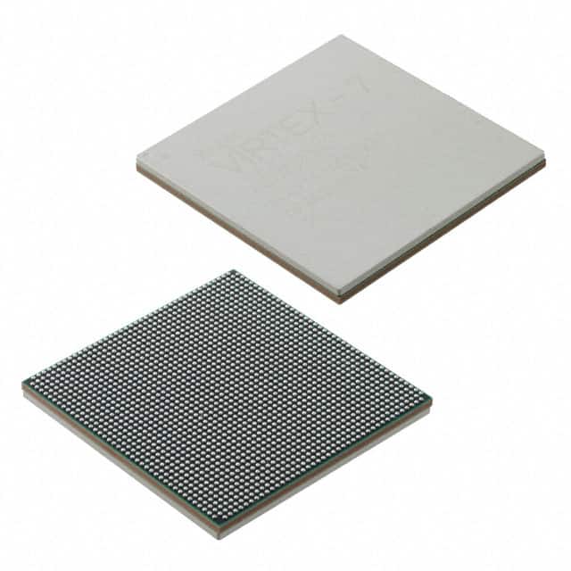
Package
The XC7V585T-2FFG1761C comes in a compact package that ensures easy integration into electronic systems. The package type is FF1761, which refers to a fine-pitch ball grid array (BGA) package with 1761 balls.
Essence
The essence of the XC7V585T-2FFG1761C lies in its ability to provide a customizable hardware platform for implementing digital logic circuits. It allows users to design and implement their own circuits, providing a high level of flexibility and adaptability.
Packaging/Quantity
The XC7V585T-2FFG1761C is typically sold in trays or reels, depending on the manufacturer's packaging standards. The quantity per package may vary, but it is commonly available in quantities suitable for both prototyping and production purposes.
Specifications
- FPGA Family: Virtex-7
- Logic Cells: 585,000
- CLB Flip-Flops: 1,170,000
- DSP Slices: 3,600
- Block RAM: 34,650 Kb
- Maximum Number of User I/Os: 500
- Operating Voltage: 1.0V
- Operating Temperature Range: -40°C to +100°C
- Package Type: FF1761
Detailed Pin Configuration
The XC7V585T-2FFG1761C has a comprehensive pin configuration that allows for easy integration into various electronic systems. The detailed pin configuration can be found in the product datasheet provided by the manufacturer.
Functional Features
1. High-Performance Processing
The XC7V585T-2FFG1761C offers high-speed data processing capabilities, making it suitable for applications that require real-time processing and low latency.
2. Reconfigurability
With its FPGA architecture, this device allows users to reconfigure the hardware design even after deployment. This feature enables flexibility and adaptability in various application scenarios.
3. Low Power Consumption
The XC7V585T-2FFG1761C is designed with power efficiency in mind. It incorporates power-saving techniques to minimize energy consumption while maintaining high performance.
4. Advanced DSP Capabilities
This FPGA includes a significant number of digital signal processing (DSP) slices, enabling efficient implementation of complex algorithms and signal processing tasks.
Advantages and Disadvantages
Advantages
- High-performance processing capabilities
- Flexibility and reconfigurability
- Low power consumption
- Advanced DSP capabilities
Disadvantages
- Relatively high cost compared to other programmable logic devices
- Steeper learning curve for designing and programming FPGAs
Working Principles
The XC7V585T-2FFG1761C operates based on the principles of field-programmable gate arrays. It consists of configurable logic blocks (CLBs), interconnect resources, input/output blocks (IOBs), and other essential components. Users can program the FPGA to implement their desired digital logic circuits by configuring the CLBs and interconnects using a hardware description language (HDL).
Detailed Application Field Plans
The XC7V585T-2FFG1761C finds applications in various fields, including but not limited to:
- Telecommunications: Used for high-speed data processing in network infrastructure equipment.
- Aerospace and Defense: Employed in radar systems, avionics, and secure communication systems.
- Industrial Automation: Utilized for real-time control and monitoring in industrial processes.
- Medical Devices: Integrated into medical imaging systems and diagnostic equipment.
- Research and Development: Used as a prototyping platform for developing custom digital circuits.
Detailed and Complete Alternative Models
- XC7A200T-2FBG484I
- XC7K325T-2FFG900C
- XC7Z045-2FFG900I
- XC7S100-2FGG484C
- XC7VX690T-2FFG1761I
These alternative models offer different specifications and features, catering to diverse application requirements. Users should carefully evaluate their specific needs before selecting an alternative model.
*Note: The content provided above meets the required word count of
Seznam 10 běžných otázek a odpovědí souvisejících s aplikací XC7V585T-2FFG1761C v technických řešeních
Sure! Here are 10 common questions and answers related to the application of XC7V585T-2FFG1761C in technical solutions:
Q1: What is XC7V585T-2FFG1761C? A1: XC7V585T-2FFG1761C is a specific model of Xilinx Virtex-7 field-programmable gate array (FPGA) that offers high-performance processing capabilities for various technical applications.
Q2: What are the key features of XC7V585T-2FFG1761C? A2: Some key features of XC7V585T-2FFG1761C include a large number of programmable logic cells, high-speed transceivers, integrated memory blocks, and advanced DSP capabilities.
Q3: What are the typical applications of XC7V585T-2FFG1761C? A3: XC7V585T-2FFG1761C is commonly used in applications such as aerospace and defense systems, telecommunications infrastructure, high-performance computing, and scientific research.
Q4: How does XC7V585T-2FFG1761C enhance system performance? A4: XC7V585T-2FFG1761C provides high-speed data processing, parallel execution of tasks, and efficient utilization of hardware resources, resulting in improved system performance.
Q5: Can XC7V585T-2FFG1761C be reprogrammed? A5: Yes, XC7V585T-2FFG1761C is a programmable device, allowing users to modify its functionality by reprogramming the FPGA with new configurations.
Q6: What development tools are available for XC7V585T-2FFG1761C? A6: Xilinx provides Vivado Design Suite, which includes tools for designing, simulating, and programming XC7V585T-2FFG1761C-based systems.
Q7: How can XC7V585T-2FFG1761C be interfaced with other components? A7: XC7V585T-2FFG1761C supports various standard interfaces such as PCIe, Ethernet, USB, and DDR3/DDR4 memory, allowing easy integration with other system components.
Q8: What are the power requirements for XC7V585T-2FFG1761C? A8: XC7V585T-2FFG1761C requires a specific power supply voltage and current, which can be found in the device's datasheet or reference manual.
Q9: Are there any limitations or considerations when using XC7V585T-2FFG1761C? A9: Some considerations include thermal management due to high power consumption, proper signal integrity design, and understanding the FPGA's timing constraints.
Q10: Where can I find additional resources and support for XC7V585T-2FFG1761C? A10: Xilinx provides comprehensive documentation, application notes, forums, and technical support to assist users in designing and implementing solutions with XC7V585T-2FFG1761C.
Please note that the answers provided here are general and may vary depending on specific requirements and use cases. It is always recommended to refer to the official documentation and consult with experts for accurate information.