

Viz Specifikace pro podrobnosti o produktu.
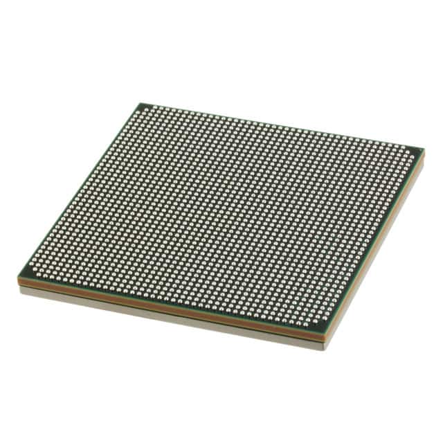
XC7VX690T-2FFG1926C
Product Overview
Category
The XC7VX690T-2FFG1926C belongs to the category of Field-Programmable Gate Arrays (FPGAs).
Use
FPGAs are integrated circuits that can be programmed and reprogrammed to perform various digital functions. The XC7VX690T-2FFG1926C is specifically designed for high-performance applications that require complex logic and processing capabilities.
Characteristics
- High-performance FPGA with advanced features
- Large capacity and high-speed processing capabilities
- Flexible and reconfigurable design
- Suitable for demanding applications in industries such as telecommunications, aerospace, and defense
Package
The XC7VX690T-2FFG1926C comes in a Flip-Chip Fine-Pitch Ball Grid Array (FFG) package.
Essence
The essence of the XC7VX690T-2FFG1926C lies in its ability to provide a highly customizable and powerful platform for implementing complex digital systems.
Packaging/Quantity
The XC7VX690T-2FFG1926C is typically packaged individually and is available in varying quantities depending on the manufacturer or distributor.
Specifications
- FPGA Family: Virtex-7
- Logic Cells: 1,006,800
- CLB Flip-Flops: 3,015,600
- DSP Slices: 3,600
- Block RAM: 54 Mb
- Maximum I/O Pins: 1,920
- Operating Voltage: 0.95V - 1.05V
- Operating Temperature: -40°C to 100°C
- Package Type: FFG1926
Detailed Pin Configuration
The detailed pin configuration of the XC7VX690T-2FFG1926C can be found in the manufacturer's datasheet or technical documentation. It provides information on the specific functions and connections of each pin.
Functional Features
The XC7VX690T-2FFG1926C offers several functional features that make it suitable for high-performance applications:
- High Logic Capacity: With over 1 million logic cells, the FPGA can handle complex digital designs.
- High-Speed Processing: The FPGA supports high-speed data processing and can operate at frequencies up to several hundred megahertz.
- Reconfigurability: The FPGA can be reprogrammed multiple times, allowing for flexibility in design iterations and system upgrades.
- DSP Slices: The integrated Digital Signal Processing (DSP) slices enable efficient implementation of signal processing algorithms.
- Block RAM: The large on-chip memory resources provide fast and efficient data storage capabilities.
Advantages and Disadvantages
Advantages
- High performance and processing capabilities
- Flexibility and reconfigurability
- Large logic capacity and memory resources
- Suitable for demanding applications
Disadvantages
- Higher cost compared to other programmable logic devices
- Steeper learning curve for programming and design
Working Principles
The XC7VX690T-2FFG1926C operates based on the principles of configurable logic and interconnects. The FPGA consists of an array of configurable logic blocks (CLBs), interconnected by a network of programmable routing resources. The configuration of these blocks and interconnects determines the functionality of the FPGA.
During operation, the FPGA is programmed using a Hardware Description Language (HDL) or a graphical design tool. The desired digital circuit is described using the HDL, which is then synthesized and implemented onto the FPGA. The configured FPGA can then perform the specified digital functions.
Detailed Application Field Plans
The XC7VX690T-2FFG1926C finds applications in various fields that require high-performance digital processing capabilities. Some of the detailed application field plans include:
- Telecommunications: The FPGA can be used in base stations, routers, and network switches to handle high-speed data processing and protocol conversion.
- Aerospace and Defense: It can be employed in radar systems, avionics, and military communication equipment for real-time signal processing and data encryption.
- High-Performance Computing: The FPGA can accelerate computationally intensive tasks in scientific simulations, data analytics, and artificial intelligence applications.
- Image and Video Processing: It can be utilized in medical imaging, video surveillance, and multimedia systems for real-time image and video processing.
Detailed and Complete Alternative Models
Some alternative models to the XC7VX690T-2FFG1926C with similar capabilities and features include:
- Xilinx Virtex-7 XC7VX485T-2FFG1761C
- Altera Stratix V 5SGXEA7N2F45C2
- Intel Cyclone 10 GX 10CX220YF780
Seznam 10 běžných otázek a odpovědí souvisejících s aplikací XC7VX690T-2FFG1926C v technických řešeních
Sure! Here are 10 common questions and answers related to the application of XC7VX690T-2FFG1926C in technical solutions:
Question: What is XC7VX690T-2FFG1926C?
- Answer: XC7VX690T-2FFG1926C is a high-performance field-programmable gate array (FPGA) manufactured by Xilinx.Question: What are the key features of XC7VX690T-2FFG1926C?
- Answer: Some key features include a large number of programmable logic cells, high-speed transceivers, integrated memory blocks, and advanced DSP capabilities.Question: What are the typical applications of XC7VX690T-2FFG1926C?
- Answer: XC7VX690T-2FFG1926C is commonly used in applications such as telecommunications, aerospace, defense, high-performance computing, and video processing.Question: What is the maximum operating frequency of XC7VX690T-2FFG1926C?
- Answer: The maximum operating frequency of XC7VX690T-2FFG1926C is typically around 800 MHz to 1 GHz, depending on the design and implementation.Question: How much programmable logic capacity does XC7VX690T-2FFG1926C offer?
- Answer: XC7VX690T-2FFG1926C provides approximately 2 million logic cells, making it suitable for complex and highly parallel designs.Question: Can XC7VX690T-2FFG1926C support high-speed serial communication protocols?
- Answer: Yes, XC7VX690T-2FFG1926C includes multiple high-speed transceivers that can support protocols like PCIe, Ethernet, and Serial RapidIO.Question: Does XC7VX690T-2FFG1926C have built-in memory resources?
- Answer: Yes, XC7VX690T-2FFG1926C has integrated memory blocks (BRAM) that can be used for data storage or as lookup tables.Question: What are the power requirements for XC7VX690T-2FFG1926C?
- Answer: The power requirements vary depending on the specific implementation, but typically XC7VX690T-2FFG1926C operates at around 1.0V core voltage and requires additional voltages for I/O banks.Question: Can XC7VX690T-2FFG1926C be reprogrammed after deployment?
- Answer: Yes, XC7VX690T-2FFG1926C is a field-programmable device, meaning it can be reprogrammed even after it has been deployed in a system.Question: Are there any development tools available for programming XC7VX690T-2FFG1926C?
- Answer: Yes, Xilinx provides a suite of development tools, including Vivado Design Suite, which allows designers to program and debug XC7VX690T-2FFG1926C efficiently.
Please note that the answers provided here are general and may vary based on specific design requirements and implementation details.