

Viz Specifikace pro podrobnosti o produktu.
XCV100-4BG256I
Product Overview
Category
The XCV100-4BG256I belongs to the category of Field Programmable Gate Arrays (FPGAs).
Use
FPGAs are integrated circuits that can be programmed and reprogrammed to perform various digital functions. The XCV100-4BG256I is specifically designed for applications requiring high-performance logic integration.
Characteristics
- High-performance FPGA with advanced programmability
- Offers a wide range of logic elements and I/O capabilities
- Provides flexibility in designing complex digital systems
- Supports rapid prototyping and development cycles
Package
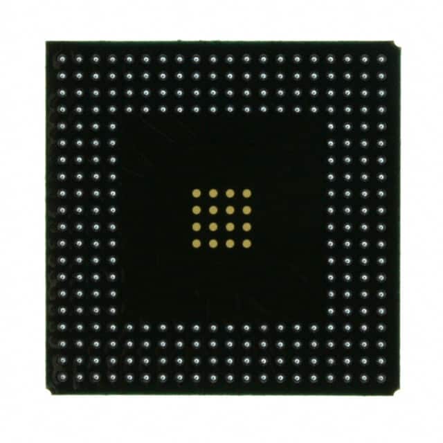
The XCV100-4BG256I comes in a 256-ball grid array (BGA) package.
Essence
The essence of the XCV100-4BG256I lies in its ability to provide a customizable and reconfigurable hardware platform for implementing digital designs.
Packaging/Quantity
The XCV100-4BG256I is typically packaged individually and is available in various quantities depending on the customer's requirements.
Specifications
- Logic Cells: 100,000
- Flip-Flops: 4,000
- Block RAM: 4,608 bits
- Maximum Frequency: 250 MHz
- Operating Voltage: 1.8V
- I/O Standards: LVCMOS, LVTTL, HSTL, SSTL, LVDS
Detailed Pin Configuration
The XCV100-4BG256I has a total of 256 pins arranged in a grid array configuration. Each pin serves a specific function, including input, output, or power supply. For a detailed pin configuration diagram, please refer to the product datasheet.
Functional Features
- High logic capacity allows for complex digital designs
- Flexible I/O options support various interface standards
- Advanced programmability enables rapid prototyping and iterative development
- Efficient power management features for optimized energy consumption
- Built-in security features to protect intellectual property
Advantages and Disadvantages
Advantages
- Versatile and customizable hardware platform
- High-performance logic integration
- Rapid prototyping and development cycles
- Energy-efficient design
- Enhanced security features
Disadvantages
- Steep learning curve for beginners
- Higher cost compared to traditional fixed-function integrated circuits
- Limited analog functionality compared to dedicated analog devices
Working Principles
The XCV100-4BG256I utilizes a matrix of configurable logic blocks (CLBs) interconnected through programmable routing resources. These CLBs can be programmed to implement various digital functions, such as arithmetic operations, memory storage, and control logic. The configuration of the FPGA is stored in on-chip memory elements, allowing for reprogramming as needed.
Detailed Application Field Plans
The XCV100-4BG256I finds applications in a wide range of fields, including:
- Telecommunications: Used in base stations, network switches, and routers for high-speed data processing.
- Aerospace and Defense: Employed in radar systems, avionics, and secure communication equipment.
- Industrial Automation: Utilized in control systems, robotics, and machine vision applications.
- Medical Devices: Integrated into medical imaging systems, patient monitoring devices, and laboratory equipment.
- Automotive: Applied in advanced driver-assistance systems (ADAS), infotainment systems, and engine control units.
Detailed and Complete Alternative Models
- XCV50-4BG256I: A lower-capacity FPGA with 50,000 logic cells, suitable for smaller-scale designs.
- XCV200-6BG432I: A higher-capacity FPGA with 200,000 logic cells, ideal for complex and demanding applications.
- XCV400-8FG900I: A larger FPGA with 400,000 logic cells and additional features for high-performance computing.
These alternative models offer varying levels of logic capacity and performance to cater to different design requirements.
In conclusion, the XCV100-4BG256I is a high-performance FPGA that provides flexibility, programmability, and advanced integration capabilities. Its versatile nature makes it suitable for a wide range of applications across various industries.
Seznam 10 běžných otázek a odpovědí souvisejících s aplikací XCV100-4BG256I v technických řešeních
Sure! Here are 10 common questions and answers related to the application of XCV100-4BG256I in technical solutions:
Q: What is the XCV100-4BG256I? A: The XCV100-4BG256I is a field-programmable gate array (FPGA) manufactured by Xilinx.
Q: What are the key features of the XCV100-4BG256I? A: The XCV100-4BG256I offers 100,000 system gates, 4,000 logic cells, and 256-ball grid array (BGA) packaging.
Q: What applications can the XCV100-4BG256I be used for? A: The XCV100-4BG256I is commonly used in various technical solutions such as industrial automation, telecommunications, automotive electronics, and medical devices.
Q: How does the XCV100-4BG256I differ from other FPGAs? A: The XCV100-4BG256I stands out with its low power consumption, high performance, and small form factor, making it suitable for space-constrained applications.
Q: Can the XCV100-4BG256I be reprogrammed after deployment? A: Yes, the XCV100-4BG256I is a field-programmable device, meaning it can be reprogrammed even after it has been deployed in a system.
Q: What development tools are available for programming the XCV100-4BG256I? A: Xilinx provides software tools like Vivado Design Suite that enable developers to program and configure the XCV100-4BG256I.
Q: Are there any limitations to the XCV100-4BG256I's I/O capabilities? A: The XCV100-4BG256I offers 72 user I/O pins, which may be sufficient for many applications. However, if more I/O is required, a different FPGA with more pins might be needed.
Q: Can the XCV100-4BG256I interface with other components or devices? A: Yes, the XCV100-4BG256I supports various communication protocols such as SPI, I2C, UART, and Ethernet, allowing it to interface with other components or devices in a system.
Q: What are the power requirements for the XCV100-4BG256I? A: The XCV100-4BG256I typically operates at a voltage range of 1.8V to 3.3V, depending on the specific design requirements.
Q: Where can I find additional resources and support for working with the XCV100-4BG256I? A: Xilinx provides comprehensive documentation, application notes, and technical support through their website and community forums to assist developers working with the XCV100-4BG256I.