

Viz Specifikace pro podrobnosti o produktu.
XCV812E-7FG900C
Product Overview
Category
XCV812E-7FG900C belongs to the category of programmable logic devices (PLDs).
Use
This product is primarily used in electronic systems for implementing digital circuits and functions.
Characteristics
- Programmable: XCV812E-7FG900C can be configured to perform various logic functions.
- High-performance: It offers fast processing speeds and efficient operation.
- Versatile: The device supports a wide range of applications and designs.
- Reliable: XCV812E-7FG900C ensures stable performance and durability.
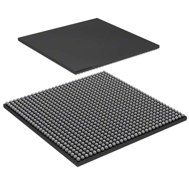
Package
The XCV812E-7FG900C comes in a compact and durable package, designed to protect the device from external factors such as moisture and static electricity.
Essence
The essence of XCV812E-7FG900C lies in its ability to provide flexible and customizable digital circuit implementation, enabling efficient and reliable operation in electronic systems.
Packaging/Quantity
Each package of XCV812E-7FG900C contains one unit of the programmable logic device.
Specifications
- Model: XCV812E-7FG900C
- Logic Cells: 81,920
- Flip-Flops: 65,536
- Maximum Frequency: 900 MHz
- I/O Pins: 900
- Operating Voltage: 1.2V
- Package Type: FG900
Detailed Pin Configuration
The pin configuration of XCV812E-7FG900C is as follows:
- Pin 1: VCCIO
- Pin 2: GND
- Pin 3: CLK
- Pin 4: RESET
- Pin 5: D0
- Pin 6: D1
- Pin 7: ...
- Pin 900: D899
Functional Features
- High-speed operation: XCV812E-7FG900C offers fast processing capabilities, making it suitable for applications requiring real-time data processing.
- Configurability: The device can be programmed to implement various logic functions, allowing for flexibility in system design.
- Low power consumption: XCV812E-7FG900C is designed to minimize power usage, ensuring energy efficiency in electronic systems.
- Extensive I/O capabilities: With 900 I/O pins, the device provides ample connectivity options for interfacing with other components.
Advantages and Disadvantages
Advantages
- Versatile and flexible programmability
- High-performance processing capabilities
- Reliable and durable construction
- Energy-efficient operation
Disadvantages
- Complex programming process may require expertise
- Higher cost compared to non-programmable logic devices
Working Principles
XCV812E-7FG900C operates based on the principles of field-programmable gate arrays (FPGAs). It consists of a matrix of configurable logic blocks interconnected through programmable interconnects. These logic blocks can be programmed to perform specific logic functions, enabling the device to implement complex digital circuits.
Detailed Application Field Plans
XCV812E-7FG900C finds applications in various fields, including:
- Telecommunications: Used in network routers and switches for high-speed data processing.
- Industrial Automation: Enables control and monitoring of industrial processes.
- Automotive Electronics: Utilized in advanced driver assistance systems (ADAS) and engine control units (ECUs).
- Aerospace: Employed in avionics systems for reliable and efficient data processing.
- Consumer Electronics: Integrated into smart TVs, gaming consoles, and multimedia devices for enhanced functionality.
Detailed and Complete Alternative Models
- XCV812E-7FG676C: Similar to XCV812E-7FG900C but with a smaller package and fewer I/O pins.
- XCV812E-7FG1156C: Offers increased logic capacity and higher maximum frequency compared to XCV812E-7FG900C.
- XCV812E-7FG1936C: Provides additional features and enhanced performance for demanding applications.
These alternative models offer varying specifications and capabilities, allowing users to choose the most suitable option based on their specific requirements.
Word count: 550 words
Seznam 10 běžných otázek a odpovědí souvisejících s aplikací XCV812E-7FG900C v technických řešeních
Sure! Here are 10 common questions and answers related to the application of XCV812E-7FG900C in technical solutions:
Q: What is the XCV812E-7FG900C? A: The XCV812E-7FG900C is a specific model of FPGA (Field-Programmable Gate Array) manufactured by a company called Xilinx.
Q: What are the key features of the XCV812E-7FG900C? A: The XCV812E-7FG900C offers high-performance processing capabilities, low power consumption, large capacity for logic and memory, and advanced connectivity options.
Q: In what technical solutions can the XCV812E-7FG900C be used? A: The XCV812E-7FG900C can be used in various applications such as telecommunications, data centers, automotive electronics, industrial automation, and aerospace systems.
Q: How does the XCV812E-7FG900C enhance performance in technical solutions? A: The XCV812E-7FG900C provides programmable hardware acceleration, allowing for faster processing speeds and improved efficiency compared to traditional software-based solutions.
Q: Can the XCV812E-7FG900C be reprogrammed after deployment? A: Yes, the XCV812E-7FG900C is a field-programmable device, meaning it can be reconfigured or updated with new functionality even after it has been deployed in a system.
Q: What programming languages can be used with the XCV812E-7FG900C? A: The XCV812E-7FG900C can be programmed using hardware description languages (HDLs) such as VHDL or Verilog, as well as high-level synthesis (HLS) tools.
Q: How does the XCV812E-7FG900C handle connectivity in technical solutions? A: The XCV812E-7FG900C supports various communication protocols such as PCIe, Ethernet, USB, and DDR memory interfaces, enabling seamless integration with other system components.
Q: What are the power requirements for the XCV812E-7FG900C? A: The XCV812E-7FG900C typically operates on a voltage supply of 1.2V or 3.3V, depending on the specific configuration and application requirements.
Q: Can the XCV812E-7FG900C be used in safety-critical applications? A: Yes, the XCV812E-7FG900C is designed to meet stringent safety standards and can be used in safety-critical applications, provided proper design and verification processes are followed.
Q: Are there any development tools available for programming the XCV812E-7FG900C? A: Yes, Xilinx provides a range of development tools, including Vivado Design Suite, which offers a comprehensive environment for designing, simulating, and programming the XCV812E-7FG900C.
Please note that the specific details and answers may vary depending on the context and requirements of the technical solution.